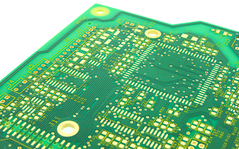
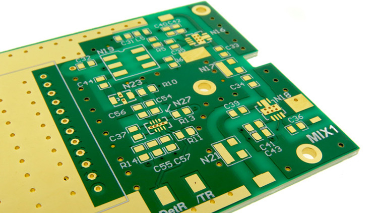
Traditionally, quick-turn printed circuit boards have been used for PCB prototyping and low-volume production in the electronics industry. Many companies have developed very low-cost, low-option Internet programs to get customers low technology printed circuit boards very inexpensively. However, in today’s evolving electronics industry, quick-turn printed circuit boards are now part of every stage of the product development lifecycle, from initial concept development to full working prototypes to getting the production product to market faster than any of their competitors.
Read MoreAs somebody whose job it is to analyze several multilayer PCB designs per week, I find it surprising whenever I receive a data package that does not include a defined lamination stack-up. The way that the layers are constructed can affect the PCBs performance, so these packages feel like they are missing a potentially important piece of information.
Read MoreHaving been involved in the printed circuit board (PCB) world for nearly four decades, I continue to see the same drawing mistakes. When declaring PCB tolerances in any given design, the PCB designer must take into consideration the manufacturing of the board itself. In this blog post, we will review some of the issues we commonly see in PCB designs that are not allowing the proper tolerances for the routing, drilling, and plating processes.
Read MoreAt the conclusion of our webinar, How PCB Design Choices Affect Overall Cost from Your PCB Fabricator, we had several questions submitted to our presenter, Ed McMahon, CEO at Epec. We have compiled these questions into a readable format on our blog.
Read MoreMany applications today send signals between two devices to provide data or to perform a specific function. These signals may consist of radio frequencies (RF) or microwave frequencies. Typically found in the communication industry, RF/microwaves are common for satellites, radar, and navigational systems. Yet, they can also be found in smaller applications, such as garage door openers, security key card terminals, wireless alarm systems, and handheld warehouse inventory scanners.
Read MoreAfter an engineer has finished their circuit design for a printed circuit board (PCB), the next step is to enter the schematic details into a computer-based schematic capture program such as Altium, Eagle, or OrCAD. The finished printed circuit board will provide the physical assembly and interconnection platform for the various electronic components required by the schematic.
Read MoreThere was a time when the PCB manufacturing industry included a fair number of bucket shops, so called because much of their processing was done in small portable tubs filled with etchants, solvents, and other mysterious solutions. They cranked out very basic, low-cost, low-complexity PCBs, using equipment and methods that were questionable at best. Their business and environmental practices were often similarly questionable.
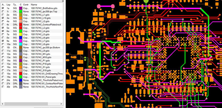
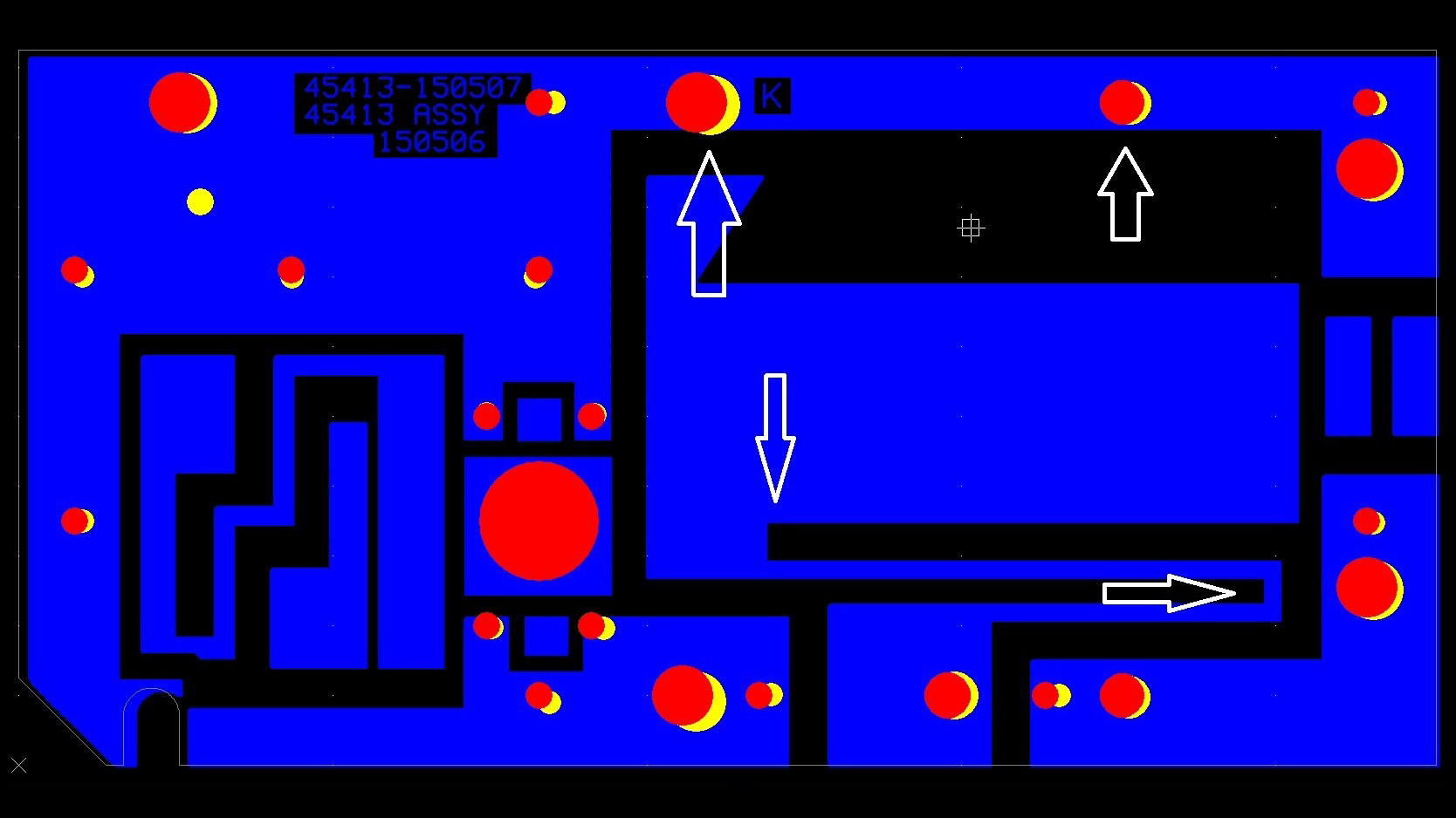
Read MoreDesign for Manufacturing (DFM) is critical to the success of your PCB order. Features that make your circuit board difficult to build add cost to your product and can increase the scrap rate. If you have designed a PCB that is more complex than usual, it is useful to submit files to your fabricator for review before placing your order so you will have some time to address any issues that might delay production.
Read MoreAt the conclusion of our recent webinar – Match Your High-Tech PCB Design To Your Supplies Capabilities – we had a number of questions for our presenter, PCB Field Applications Engineer Al Wright. We decided to compile these into a readable format on our blog.
Read MoreIn simple terms, cable assemblies are comprised of two primary elements: the conductor and the connector. Rightfully so, the conductor’s sole purpose is to pass current at a given voltage, while the connectors job is to affix the cable assembly securely to a mating interconnect.
Read More


