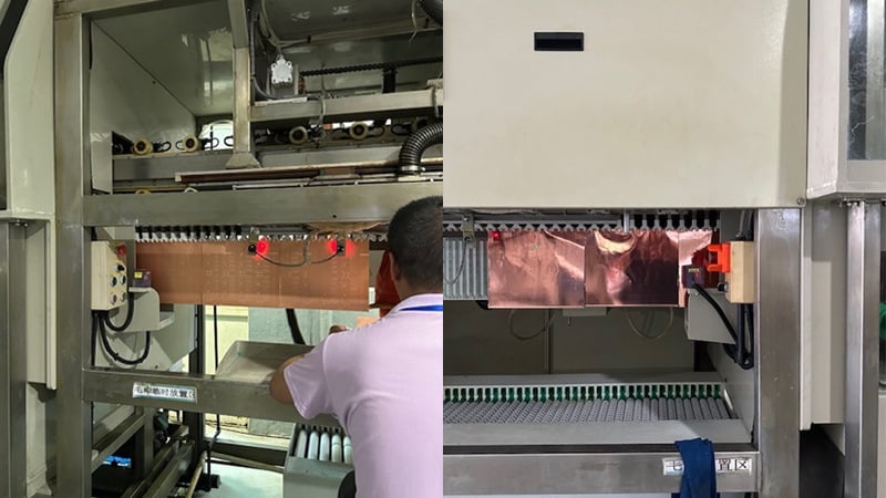
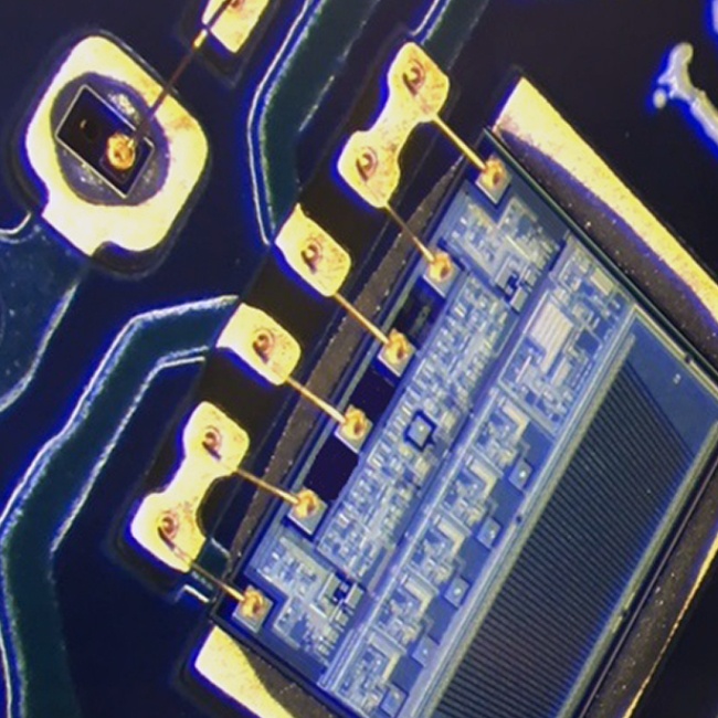
In the highly competitive world of PCB manufacturing, innovation is the key to staying ahead. The choice of manufacturing processes can significantly impact efficiency, quality, and overall production costs.
Read MoreChris Perry

Recent Posts
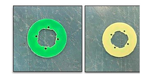
In the realm of printed circuit board (PCB) engineering, the design incorporates through holes as a means to establish connections across the board's various layers or secure the card during the assembly process. These through holes come in two distinct categories: plated and non-plated.
Read MoreThe purpose of IPC specification is to provide requirements for qualification and performance of rigid printed circuit boards based on the following constructions and/or technologies. These requirements apply to the finished product unless otherwise specified.
Read MoreENEPIG (Electroless Nickel, Immersion Palladium, Immersion Gold) was derived out of the need to combat the challenge with the immersion gold process and Black Pad Syndrome. Black Pad (the hyper corrosion of underlying nickel) was baffling both PCB assemblers and manufacturers. After much analysis, the root cause was determined to be the nickel deposit.
Read MoreSolving solderability issues for printed circuit boards (PCBs) can be a real hassle. Nothing is more frustrating than having lined up all your materials for an assembly, only to start running the package through reflow and discover that the solder paste is wetting poorly to the pads. Immediately, the profile is checked to confirm proper parameters.
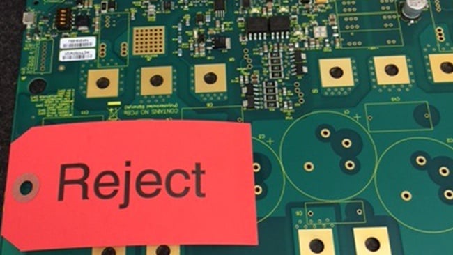
Read MoreFor customers and suppliers along the PCB manufacturing process, non-conformances will, unfortunately, happen from time to time. A non-conformance consists of receiving an order for printed circuit boards that do not meet your specifications or industry (IPC) standards. While dealing with these issues is obviously essential, the solution is sometimes not obvious and can put on-time delivery to your customer at risk. It is imperative that your circuit board supplier can deliver conforming product as soon as possible, which means having the procedures to get there.
Read MoreWith the introduction of ISO 9001:2015, which specifies requirements for quality management systems, the statement “quality management system documentation shall include a quality manual” no longer need apply. Many celebrated this as a reprieve from previously having to fully document their quality management system. However, eliminating the supplier quality manual altogether could be a dangerous takeaway on the new standard’s intention.
Read MoreI can remember the first ‘incident’ of black pad, years ago, when Epec started to use the electroless nickel immersion gold (ENIG) process. We didn’t notice the issue at the time, as it is not evident on the bare board, but received the complaint from assembly as it was later identified on completed assemblies.
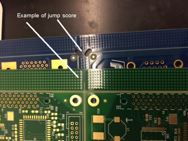
Read MoreThe V-score process is the addition of thin, double-sided cuts into printed circuit board (PCB) laminate for the purpose of assisting in the removal of individual parts from the array. The thin cuts which do not go all the way through the material, act as a perforation of the laminate so simple flexing of the laminate, or use of a cutting wheel, will aid in the removal of parts after the assembly process.
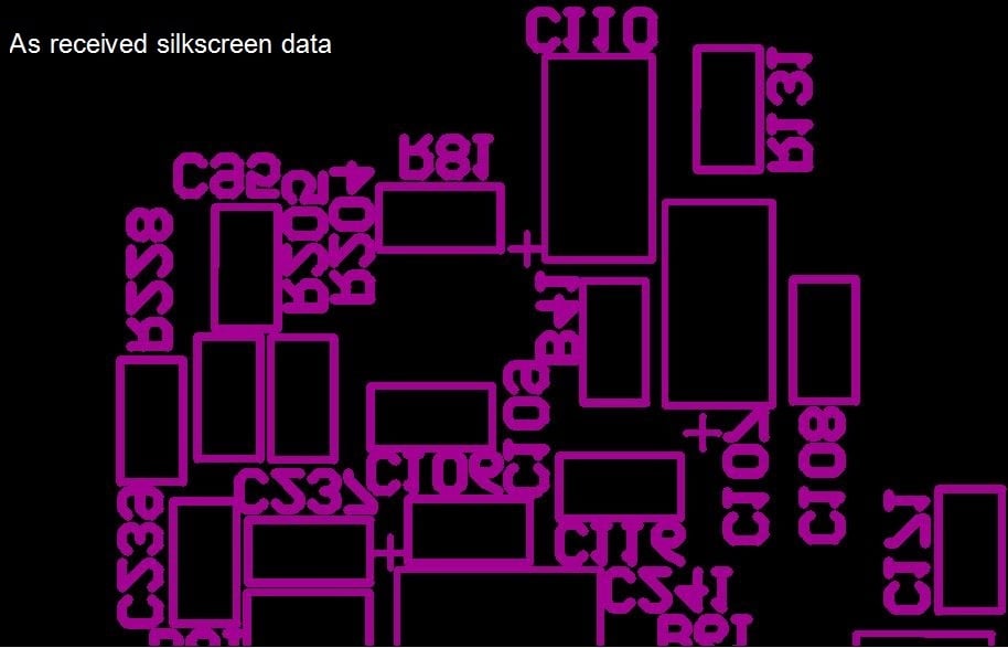
Read MoreAmong the multiple layers of a printed circuit board (PCB) lies the PCB silkscreen layer. The placement of the silkscreen markings, whether on the top or bottom layer, in conjunction with the features of the other layers, could affect the final legibility of the printed circuit board markings.
Read More


