Among the multiple layers of a printed circuit board (PCB) lies the PCB silkscreen layer. The placement of the silkscreen markings, whether on the top or bottom layer, in conjunction with the features of the other layers, could affect the final legibility of the printed circuit board markings.
Remember that PCB surface real estate is limited, so it is best to exercise caution when determining what markings to include on the PCB surface.
PCB Silkscreen Process
The PCB silkscreen process is utilized to mark nomenclature, usually on the component side of the board, though it can be on both sides.
Markings can include component locations, test points, PCB and PCBA part numbers, company logos, and UL logos or identifiers. Screen printing is done when the boards are still panelized prior to the application of the final finish or routing/v-scoring.
How to Handle Silkscreen on a Busy Surface Mount Design
As surface mount circuit boards get busier and busier, and packages get smaller, increased amounts of nomenclature are required on the board surface.
When designing the circuit board, consideration is rarely given to the character font size and location when overlaid to solderable surfaces. Designers should avoid placing nomenclature on top of circuit pads, avoid using excessively tiny text and should allow for registration tolerances.
When data is received that has nomenclature on top of circuit pads, a process known as clipping is enacted, usually by the engineering software used to set the data up for production. Markings on top of circuit pads are violations and are automatically removed by the software. Based on the amount of violations, the end result may not be favorable for legibility, but necessary for functionality.
Below is an example of “as received” marking data. As can be observed, the character spacing is already quite tight.
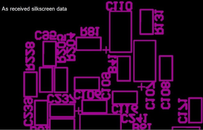
Received Printed Circuit BoardSilkscreen Data
Now we take the same layer and overlay it to the copper image. At any point that the markings come in contact with the red areas, it is an IPC violationn and the non-conforming marking area will be removed. This “clipping” process is performed automatically by the engineering software.
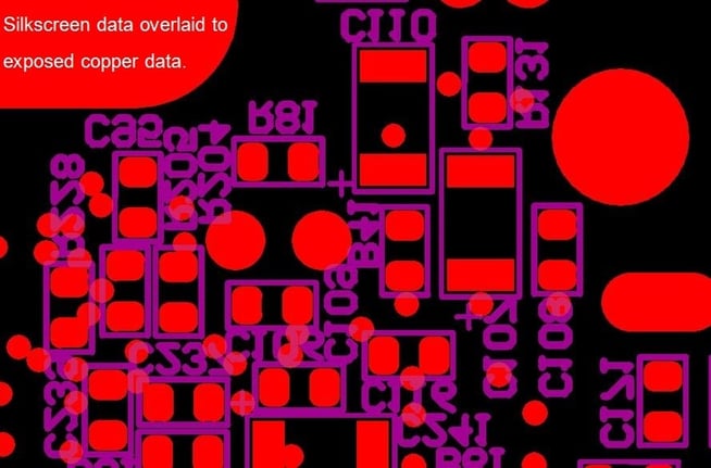
Printed Circuit Board Silkscreen Data Overlaid to Exposed Copper Data
After the clipping process, depending on the amount of clipping performed, the end result could be undesirable. Below is an example of data after the clipping process.

Clipped Printed Circuit Board Silkscreen in Data
After clipping, based on the number of violations, the legibility of the remaining markings on the actual parts can be challenging, as the below photo shows.
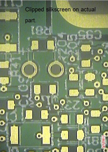
Clipped Printed Circuit Board Silkscreen on Actual Part
So, The Question Becomes…
Do the parts violate IPC for marking legibility when the root cause of the poor PCB silkscreen legibility issue is clipping of the marking data?
In theory, the answer would be no as the clipping of the silkscreen is design driven. The legibility of the silkscreen also does not affect board functionality whereas marking ink on solderable surfaces has a high negative impact on functionality.
Incoming inspection needs to be aware of marking locations in relation to solderable surfaces when determining silkscreen legibility. However, the printed circuit board supplier should also inform their customer when their received data incurs extreme clipping of the silk screen and offer a resolution.
Summary
Poor silkscreen legibility on PCBs is often the result of a necessary process called clipping, where any silkscreen data overlapping solderable pads is automatically removed to meet IPC standards. While clipping ensures board functionality by preventing ink contamination on pads, it can significantly reduce the readability of markings on dense, surface-mount designs. Since legibility does not impact functionality, clipped silkscreens do not violate IPC, but suppliers should communicate with customers when extreme clipping occurs and propose adjustments to improve clarity in future designs.
Key Takeaways
- Silkscreen purpose: Used to mark component locations, test points, part numbers, and logos, typically applied before final finishing.
- Design constraints: Overcrowded layouts, tiny text, and silkscreen over pads lead to clipping during the setup process.
- Clipping necessity: Engineering software automatically removes markings overlapping solderable surfaces to maintain board functionality.
- Impact on legibility: Excessive clipping can leave silkscreens difficult to read, though this does not constitute an IPC violation.
- Best practices: Designers should avoid placing text on pads, allow for registration tolerances, and suppliers should alert customers when silkscreen clarity is heavily compromised.


