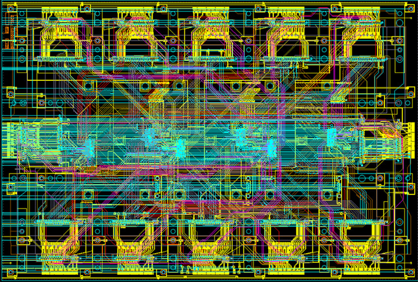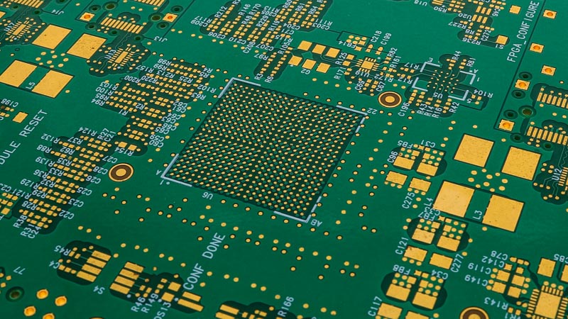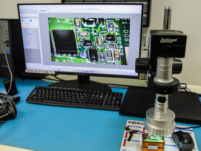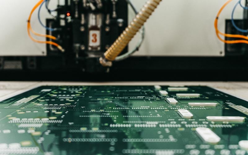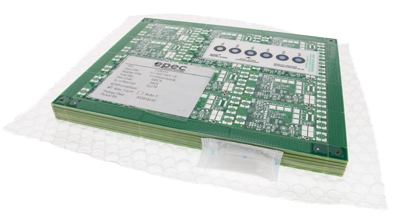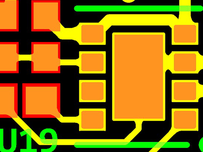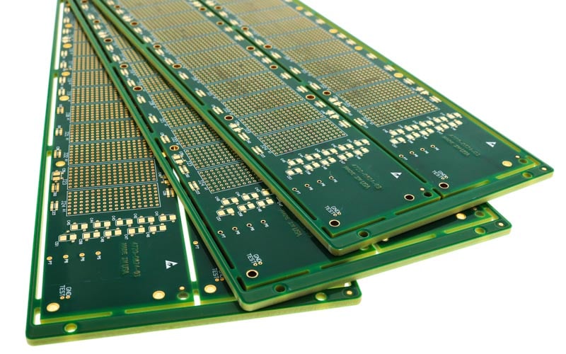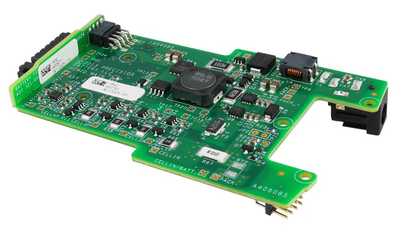

A great tool to catch printed circuit board (PCB) defects before they cause problems is the ability to identify process indicators. The earlier these process indicators can be identified in the PCB fabrication process, the greater the ability to avoid financial risk with the PCB builds. In high-reliability applications, waiting until final inspection to catch defects is too late. By that point, time, materials, and labor have already been invested, and the cost of rework or scrap can be high.
Read MoreAt the conclusion of our webinar, Navigating PCB Supply Chain Challenges, we had several questions submitted to our presenter, Epec President Kendall Paradise. We compiled these into a readable format on our blog.
Read MorePrinted circuit board (PCB) manufacturing relies on a coordinated combination of materials and processes to create reliable electronic circuits. Insulating substrates like FR-4 fiberglass-epoxy or specialized polymers provide mechanical strength and electrical isolation, while conductive copper layers are patterned using photoresists and chemical etchants.
Read MoreFrom a PCB manufacturing perspective, designing for testability focuses on ensuring the circuit board can be efficiently inspected and verified at scale without slowing down production or increasing costs.
Read MoreIn today’s high-density electronics, designers are constantly balancing miniaturization with long-term reliability. One technology that makes compact layouts possible is the use of blind and buried vias, specialized interconnections that don’t completely pass through the board like traditional plated-through-holes.
Read MoreMany engineers and buyers assume that printed circuit board (PCB) manufacturers are only interested in large production volume orders. It is an easy conclusion to draw. High-volume manufacturing often dominates industry conversations, and many suppliers structure their operations around scale. But the reality is very different for companies like Epec, which specializes in high mix, low/medium volume-engineered products like PCBs.
Read MorePrinted circuit board assemblies used inside battery packs operate in a uniquely demanding environment. They are often enclosed, exposed to temperature swings, subjected to charge and discharge cycles, and expected to perform reliably for years without service.
Read MoreWhen a printed circuit board (PCB) overheats in the field, the root cause often traces back to one simple question that was never fully answered during layout: how much current is really flowing through each trace? Trace sizing and copper weight decisions may seem routine, but small assumptions at this stage can lead to voltage drop, excessive heat, and long-term reliability problems.
Read MorePrinted circuit board (PCB) field failures are among the costliest issues electronics companies face. A circuit board that performs perfectly in the initial testing process but fails in the field can be catastrophic. Performing design-for-manufacturability (DFM) on the PCB data before production manufacturing begins prevents oversights that could have been prevented early in the product lifecycle.
Read MoreEffective thermal management is a crucial aspect of multilayer printed circuit board fabrication. As circuit density and power requirements continue to increase, so does the potential for heat buildup within a board’s layers. Without proper control, excessive temperatures can cause delamination, warping, component failure, and signal instability.
Read More