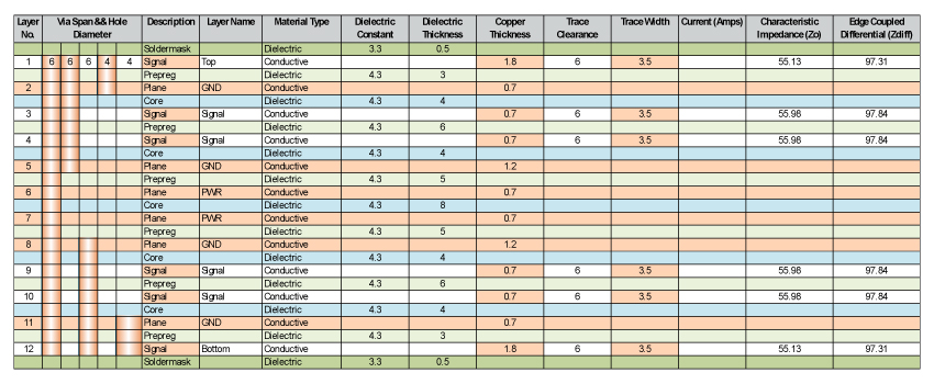
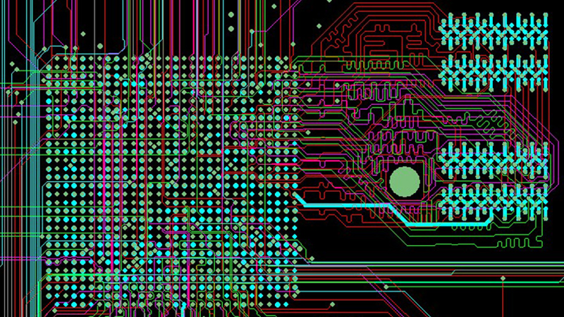
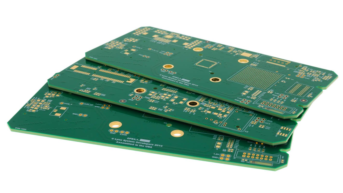
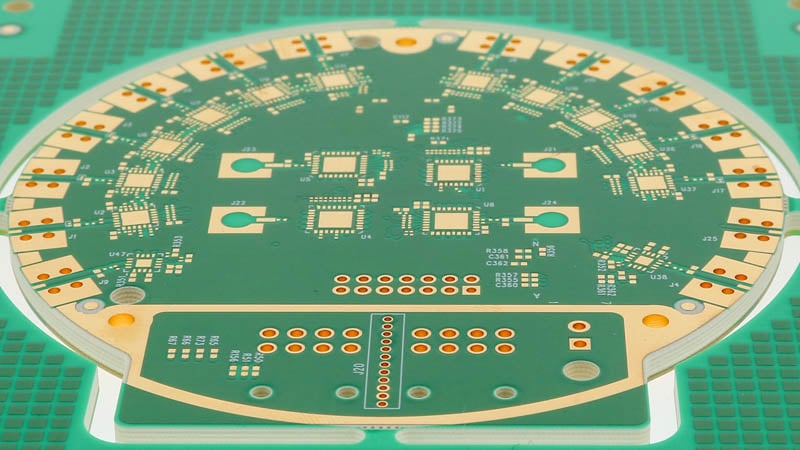
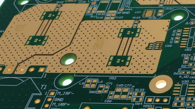
When a printed circuit board (PCB) overheats in the field, the root cause often traces back to one simple question that was never fully answered during layout: how much current is really flowing through each trace? Trace sizing and copper weight decisions may seem routine, but small assumptions at this stage can lead to voltage drop, excessive heat, and long-term reliability problems.
Read MoreAngie Brown

Recent Posts
Printed circuit board (PCB) field failures are among the costliest issues electronics companies face. A circuit board that performs perfectly in the initial testing process but fails in the field can be catastrophic. Performing design-for-manufacturability (DFM) on the PCB data before production manufacturing begins prevents oversights that could have been prevented early in the product lifecycle.
Read MoreIt’s no secret that as printed circuit boards (PCBs) have evolved into higher technology levels, it has become more difficult to process the boards in a standard production setting. By standard, I mean panelized boards popped onto the line or conveyor and letting them run. Copper is the driving processing factor for a lot of production; the ounce weight drives the part and determines how long.
Read MoreI have spoken in the past about my long career in printed circuit board (PCB) manufacturing (1982) and how, at the beginning of my career, we still had home phones tied to the wall by cord. If we were lucky enough, the spiral stretch cord was very long.
Read MoreIn modern electronic systems, the need for high-speed data transmission has never been greater. With faster clock speeds, smaller geometries, and increasing complexity in printed circuit board (PCB) layouts, ensuring signal integrity has become a top priority for designers. Consulting your PCB manufacturer should be at the top of your list.
Read MorePrototyping is one of the most critical stages in the development of any electronic product. A well-designed printed circuit board (PCB) prototype can help you validate your concept, detect flaws early, and streamline the transition to production.
Read MoreWhen I first started thinking about printed circuit board (PCB) testing, my immediate reaction was boredom. Let’s be honest, it doesn’t have the hands-on excitement of building the circuit board itself. You're not designing the PCB; you're just running it through a tester, sorting it into a pass or fail bin, and moving on. I’ve done the job myself, so I know how repetitive it can feel.
Read MoreThe subject here isn’t all that glamorous, however, the requests about high-frequency printed circuit board (PCB) have increased significantly, which makes me think we have more that can be said on the subject of high-frequency applications
Read MoreWhen it comes to high-power printed circuit boards (PCBs), they require more of what we have been talking about. High-power PCBs are what is in their name, meaning they require more current than standard PCBs.
Read MoreAlthough it may not feel like it, the PCB manufacturing industry is approaching its 100th anniversary – a remarkable milestone. It’s hard for me to believe, especially having spent 40 years in the business myself. The idea of reaching a century of innovation in this field once seemed impossible. It almost feels like we should begin the story with, “A long time ago, in the 1930s,” when PCBs first came to light during WWII. Yet here we are, on the brink of celebrating this incredible achievement.
Read More


