


At the base of all printed circuit boards is the material. We have to start somewhere, so, let’s talk about the material. PCBs are built-to-print products, and although they are very similar, no matter the shape, size, or layer count, they are unique and have their attributes.
When we start our review to quote, we look at the laminate material that is called out as one of the first costing items. Keywords like FR4, 170tg, IPC-4101, or a stack-up without a suggestion will leave it up to us to determine what to use.
With so many flavors and types of materials, not all are readily available, UL-approved, or in our wheelhouse. We have a sweet spot like everyone else in the production of PCBs, and not all materials are commonly stocked.
During the design phase of your product, consider consulting your manufacturing team and ask our engineering team if what you are thinking of using is something we use. Review the data sheet and ask about our commonly stocked product. Stay away from calling our specific brands of material, like Rogers or Isola, and leave the room using an alternative by adding the word of manufacturing equivalent to your preferred. When possible, keep it simple and let us determine which material to use. Supply an overall thickness and impedance values/layers to be met with tolerance and leave the specified dielectrics to us.

Unbalanced Copper
Copper weights should always be specified as to the desired weight in ounces for the inner layers and finished copper outer layers. Internal layers do not receive additional plated copper, so the start weight is the finished weight.
The external layer has a base copper plus plating. Copper ounces should be balanced on cores, when possible, a core is a piece of laminate that is covered on two sides with copper. For example, a 6-layer PCB uses 2 cores comprised of layers 2-3 and layers 4-5, the copper on both sides of the core. When it matches 1oz. to 1oz, it creates a balance and allows the core to remain flat. When the core is unbalanced using 0.5oz./1oz., the material will tend to bow and potentially cause warp and twisting of the part.
Adding Blind and Buried Vias
Often when designing a PCB, we underestimate the land. Like everything, size matters, and with a PCB it is the same, relative to the end product. As the design group runs low on land-to-place components, one item they look at is adding blind vias to component areas or buried vias internally both add cost.
The blind or buried via process will increase the cost by 20-50% depending on the number of sets and from and to layers applied the cost can climb. The part will make multiple loops through the drilling, plating, imaging, and lamination process to complete the PCB. In many cases, it is more cost-effective to add more layers to the part to reduce these types of holes than to add this technology.
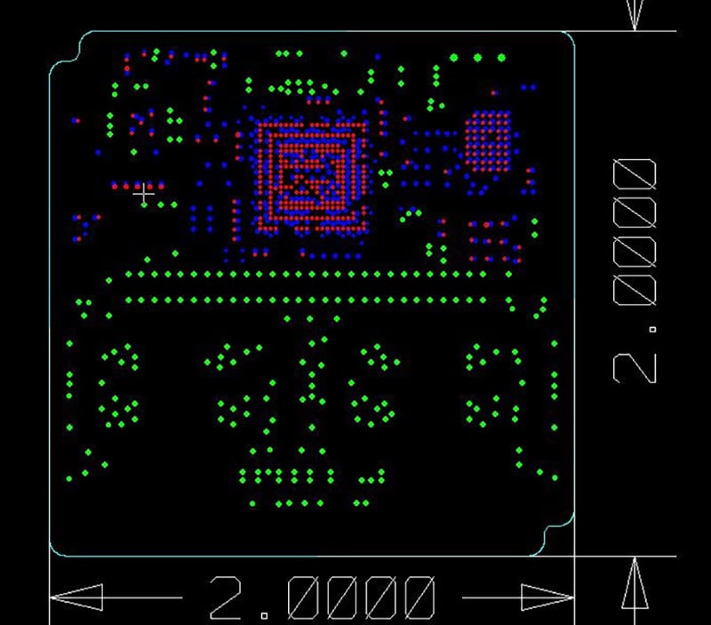
Blind/buried vias add cost. In this image, there are 2 sets of blind or buried vias as well as 1 set of through holes which equals 3 trips to the drilling/plating/imaging and other steps to complete.
Mask Color and Silkscreen Characteristics
Most of us are visually stimulated, and if a part or product catches our eye, we are more likely to buy it. PCBs can be produced in many different colors, and why color is important in a PCB, I have no idea really. I have seen many different colors that are standard and requested to build and also non-standard such as pink, magenta, purple, orange, or even sky blue. These colors, although cool, are not common and in many cases not available as standard. Like most “paint,” the base colors can be mixed to create these other colors.
The bigger problem becomes repeating the color from run to run. There is a “mixture” ratio, however, it depends on the people factor on how close the color will be to the prior run. Variance happens, and in many cases, we question the change. Being clear on the quote that the color between lots may vary is critical. Choosing the most common colors such as green, red, black, blue is best. On tight pitch or heavier copper using green is best.
For ease of assembly, a silk screen legend is needed as a roadmap to component placement. The legend, to be helpful, needs to fit certain criteria. Whether wet print or digital print, the character width and height as well as placement is critical to legibility. The minimum line width should be 0.005” or greater. With this in mind, the character height must match and be 0.035” or greater. Characters should be carefully placed to avoid copper areas using the mask as a guide. To clear mask off of copper, the minimum over size is 0.004” total or 0.002” on each side of the feature to a preferrable 0.006” total or 0.003” on all sides. The legend can then be pulled back away from copper an additional 0.001” from the mask clearance edge. When clipping legend, the characters can be left illegible, causing yet another issue for assembly. Keeping the parameters in mind during design and layout will leave a clear road map for assembly.
Legend or silkscreen as shown is difficult or impossible to process. With multiple line widths and character sizes, this makes printing nearly impossible to be legible. As you can see from the Gerber data, some areas are already blurred.
Summary
When you think about your ideas for a product, or for future revisions of an existing product, consulting with your PCB supplier on current known challenges can help. New product or new revision, using valuable resources such as Epec’s always-free DFM service can save time, cost, and production challenges. Design for manufacturing at the processing level will give you true analysis of potential pitfalls. Trusting our team to support you as a valued customer is our goal. Purchasing your stencil needs through your PCB manufacturer guarantees a problem free transition. We continue to push towards a successful future for Epec, our customers and our consumers.
Key Takeaways
- Material selection impacts cost and manufacturability: Specifying uncommon laminates or proprietary brands can delay production and raise costs. Instead, define thickness, impedance, and performance requirements while leaving equivalent material choices to the manufacturer.
- Balanced copper weights prevent warpage: Keeping copper weights equal on both sides of a core minimizes bowing and twisting. Unbalanced designs, such as 0.5 oz. on one side and 1 oz. on the other, can distort the PCB during fabrication.
- Blind and buried vias add significant expense: These features can increase costs by 20–50% due to repeated drilling, plating, and lamination cycles. In many cases, adding layers is a more cost-effective alternative.
- Mask and silkscreen choices affect quality and assembly: While unusual solder mask colors may look appealing, they are harder to reproduce consistently and can vary between runs. Standard colors such as green or black ensure reliability, and properly sized, positioned silkscreen characters improve assembly accuracy.
- DFM collaboration reduces errors and delays: Engaging your PCB supplier early and using services like Epec’s free DFM review helps identify potential pitfalls, clarify requirements, and avoid costly rework during production.


