Bow and twist of printed circuit boards (PCB) routinely rank among the highest levels of falsely identified non-conformance because it is perhaps the least understood. Envisioning a perfectly flat rigid circuit board as the standard is a fallacy believed by many incoming inspectors. Understanding the reasons and causes for PCB bow and twist can help resolve the issue at the board design stage.
Difference Between Bow and Twist
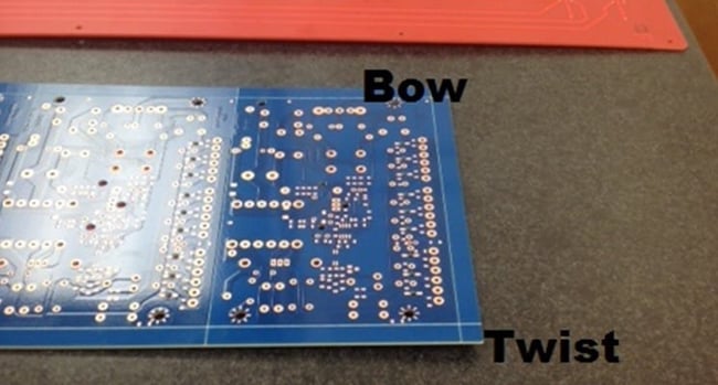
First, let’s discuss how the terms bow and twist differ. A circuit board with a bow issue will lift off the surface plate despite all four corners of the board making contact with the surface plate (imagine the shape of a bow weapon).

Example of a Printed Circuit Board with Bow and Twist
Twist occurs when three of the PCB corners are in contact with the surface plate while the fourth corner is elevated. Both conditions have requirements, per IPC, to determine if the degree of bow or twist is conforming or nonconforming.
Why Does IPC Allow For Any Bow Or Twist?
The answer is due to the materials and processes involved in printed circuit board manufacturing. PCB laminates are made with layers of fiberglass cloth and epoxy, each containing unique thermal expansion properties. Add a layer of copper to one or both sides of the PCB laminate and you must account for additional thermal expansion properties.
When the circuit board fabricator exposes the materials to various etching and thermal processes, there is no guarantee that the laminates will express uniform reaction across all samples.
Since the reaction differs from sample to sample, despite PCB laminate manufacturers following a strict fabrication process for all laminates, IPC has set an allowed tolerance. To account for normal variance, the finished product is expected to fall within defined parameters, or tolerances, rather than an exact number. These preset tolerances allow for a small degree of bow and/or twist that won't affect performance of the circuit board.
Additional Influences of Bow and Twist
Other factors affect levels of bow and twist in circuit board manufacturing, including:
- Addition of individual part number characteristics
- Higher circuit board layer counts (additional materials = additional thermal processes)
- Mixing materials (i.e. using high frequency PTFE laminate with standard FR4 to control impedance values, causing unbalanced stack-up)
- Mixing copper weights
Mixing copper weights has a negative effect on bow and twist, as copper has a high coefficient of thermal expansion. Higher density copper will expand toward the area of least resistance at greater force than a low density copper area.
A balanced stack-up allows opposing thermal expansion values to work against each other to help maintain an even bow and twist force. By unbalancing the stack-up, the side with the greater thermal expansion value will influence the complete board. Solid layers of copper plane will expand differently than signal layers, specifically if the signal density is light. Having all signals on like layers on one side of the board, with all planes on the opposite side, is a recipe for disaster.
PCB fabricators are also responsible for doing their part to ensure proper storage of raw laminates to keep materials flat, as well as the handling of work in progress to prevent production panels from being awkwardly stacked. Fabricators may also suggest copper thieving to customers when the design is susceptible to bow and twist.
Summary
Understanding PCB bow and twist provides us with parameters for acceptable standards as well as key methods of prevention. Knowing the primary causes for bow and twist of printed circuit boards is essential for manufacturers, but they do NOT eliminate the circuit board fabricator as a possible root cause. With better understanding comes a better, more effective circuit board design and manufacturing process.
Key Takeaways:
- Bow vs. Twist: Key Differences:
- Bow occurs when all four corners of a PCB touch a surface plate, but the board lifts in the middle.
- Twist occurs when three corners touch a surface plate, while the fourth does not.
- Why IPC Allows Bow and Twist:
- PCB materials (fiberglass, epoxy, and copper) have different thermal expansion properties, making perfect flatness unrealistic.
- Variations in laminate properties from lot-to-lot further impact PCB flatness.
- Design Factors Affecting Bow and Twist:
- Higher Layer Counts: More layers introduce prepreg (glue) and additional thermal processing, increasing the risk.
- Mixed Materials: Combining different laminates, like PTFE and FR4, results in uneven expansion.
- Unbalanced Stack-ups: Uneven material distribution leads to stress imbalances.
- Copper Weight and Distribution Impact:
- Uneven copper weights across layers create expansion imbalances.
- Designs with all signal layers on one side and solid copper planes on the other are prone to extreme bow and twist.
- PCB Fabricator's Role in Mitigating Bow and Twist:
- Proper laminate storage and handling to prevent material warping.
- Strategic use of copper thieving (adding copper areas to balance expansion forces) to reduce bow and twist effects.


