


Printed Circuit Boards (PCBs) are ubiquitous in today's technology-driven world, serving as the backbone for everything from smartphones to space shuttles. While they may seem straightforward, the truth is, no two PCBs are the same. With the advent of increasingly complex electronics, manufacturing PCBs has become an intricate task that involves a lot of specialized engineering.
In this blog post, we'll explore some of the less common but impactful design elements in PCBs such as different types of vias, copper-plated shut vias, and surface treatments. We'll also touch upon how these specialized processes affect both the price and the lead time of the finished product.

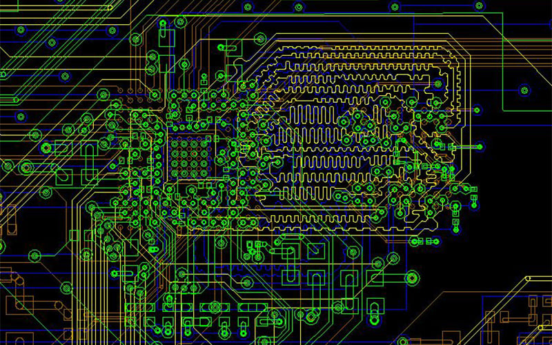
Through hole vias within BGA are precision drilling required.
The World of Vias
Blind Vias
Blind vias represent a fascinating aspect of PCB design, reflecting a subtle art form in electronic engineering. These vias are aptly named for their characteristic of being visible on only one side of the board, connecting an outer layer to hidden inner layers without penetrating the entire board.
In the past, a PCB with one or two sets of blind vias was considered complex. Today, the narrative has shifted. High-density interconnect (HDI) technology has pushed the envelope, enabling the design of smaller yet more powerful electronic devices. As a result, blind vias have become a staple in our PCB manufacturing process, with some boards incorporating up to 12 sets.
Why the increased use? The answer lies in the drive for miniaturization coupled with the need for more functionality. As devices become more compact, the real estate on a PCB becomes prime property. Blind vias offer a way to connect multiple layers without consuming the space needed for other components. They enable designers to pack more features into a smaller area, leading to the development of sleeker, more efficient electronics.
From an engineering perspective, the integration of blind vias requires precision. Drilling must be accurate to ensure connectivity without damaging adjacent layers. Moreover, the increased number of blind vias per circuit board increases the risk of errors, demanding rigorous inspection and testing protocols. The drilling process also becomes more time-consuming, as each via set may require separate attention, slowing down production and impacting throughput.
With complexity comes cost. Each additional set of blind vias introduces more stages in the manufacturing process — drilling, plating, and inspection — all of which contribute to the overall cost of the PCB. This is a critical consideration for clients who must balance the design benefits against the budgetary constraints.
To keep up with the demand for blind vias, the industry has seen significant advancements in drilling technology. Laser drilling, for instance, offers the precision required for creating these minute connections. The use of lasers has reduced the margin of error, but it also requires a substantial investment in specialized equipment.
Buried Vias
Buried vias represent a fascinating aspect of PCB design, often found in more complex or high-density circuit boards. Unlike their blind counterparts, buried vias connect internal layers without ever reaching the surface, making them invisible to the naked eye once the PCB is assembled. This hidden nature is not without its challenges; it demands non-destructive testing methods such as X-ray inspection to ensure integrity and connectivity.
The presence of buried vias is a clear indicator of a circuit board's complexity and typically implies a higher tier of electronic functionality. They allow for denser and more efficient use of the PCBs real estate by facilitating inter-layer connections without affecting the layout of the outer layers.
From an engineering standpoint, buried vias require meticulous planning and precise execution. The layers they connect must be accurately aligned during the lamination process to ensure the vias make perfect contact. This complexity requires an elevated level of engineering oversight and a detailed review process, which can impact both the manufacturing timeline and cost.
Stacked Vias
Stacked vias stand out as one of the most intricate features in PCB design, often reserved for the most complex and space-constrained circuits. These are not just any vias; they are a series of vias that are precisely aligned and stacked one atop the other through various circuit board layers. Their implementation is a testament to advanced engineering precision and is particularly useful in applications where space optimization is paramount, such as in multi-layer, high-speed circuitry.
The process of creating stacked vias is a dance of precision engineering involving several lamination cycles. Each cycle is a step where different layers of the PCB are pressed and heated to form a solid, unified board. Between these cycles, every via is carefully plated to ensure electrical continuity, filled with a non-conductive or conductive epoxy to provide structural integrity, and then planarized to create a flat surface for subsequent layers. This meticulous process ensures that each stacked via maintains a robust connection through all the layers it traverses.
The complexity of this process cannot be overstated. It requires not only state-of-the-art manufacturing equipment but also a high degree of coordination between the PCB design team and the manufacturing floor. The precision with which the vias must be aligned across layers means that any deviation, no matter how slight, can lead to a failed connection and potentially a scrapped circuit board.
From a cost perspective, stacked vias represent a significant investment. The time and labor involved in their creation, along with the required advanced machinery and materials, contribute to the overall cost of the PCB. Additionally, the increased manufacturing time and the heightened risk of production errors can further drive up expenses.
Multiple sets of blind vias and through holes require extra processing.
Specialized PCB Processes
Copper-Plated Shut Vias
The specialized service of copper-plated shut vias, a process that distinguishes us in the PCB manufacturing industry. This meticulous procedure not only requires specialized equipment that operates under tightly controlled conditions but also utilizes direct current (DC) chemistries tailored for precise plating. These strict requirements confine the operation to vias with diameters ranging from 6 to 12 mils, a specification that caters to high-density and high-reliability circuit boards.
The copper-plating process for these vias is not a quick one; it may extend to 18 hours to ensure a complete and uniform fill. However, this investment in time pays dividends in the form of structural integrity and reliability. The thorough plating process minimizes the occurrence of common via issues such as voids, which are air pockets that can lead to electrical discontinuities, or the entrapment of gases and chemistries, which could compromise the via's durability and the PCBs performance.
Beyond reducing the risk of such defects, this process enhances the thermal and electrical conductivity of the via, thereby improving the overall performance of the PCB. This is particularly critical for applications where superior electrical characteristics and heat management are essential. Furthermore, the robust nature of copper-plated shut vias can significantly extend the life of the product, making it a preferable choice for industries where longevity and reliability are paramount.
The added value of copper-plated shut vias cannot be overstated. While they may increase the upfront cost and production time, the benefits they provide, especially for high-performance electronic applications, make them a worthwhile investment for the right projects. This process exemplifies our commitment to offering advanced PCB solutions that meet the evolving needs of sophisticated electronics.
PCB Design Features That Add Cost
Jump scoring is a strategic design feature that significantly impacts both the function and manufacturing process of PCBs. It requires advanced precision programming to create a 'jump' in the score line, allowing for sections of the PCB to remain connected until they're ready to be separated after assembly. This attention to detail enhances the circuit board’s structural rigidity, minimizing the risk of damage during the handling and soldering phases. However, it demands a high level of precision from the production floor, with rigorous checks to ensure each jump is executed flawlessly. The additional time taken for programming and the increased oversight during manufacturing contribute to the overall cost.
Peelable masks serve as a protective layer over specific areas of the PCB during the plating or soldering processes, safeguarding components from contamination or solder bridging. The precision application of these masks, and the fact that they’re used less frequently in modern PCB designs, make them a unique feature that incurs additional expense. Their limited shelf life also introduces a logistical aspect to cost management, as any excess material must be used in a timely manner to avoid waste, thus carefully balancing order size with production schedules is crucial.
Surface treatments such as electrolysis nickel immersion palladium and immersion gold (ENEPIG) provide superior surface finishes that enhance the solderability and longevity of PCB connections. However, these combined surface treatments are complex and costly, reflecting the high price of precious metals used and the sophistication of the processes involved. The infrequent operation of the treatment lines due to their cost means that incorporating such finishes can also introduce longer lead times. While this may increase the upfront investment, the benefits of durability, performance, and enhanced electrical conductivity make these treatments invaluable for high-reliability applications.
Summary
In the complex world of PCB manufacturing, it’s crucial to understand that each circuit board is unique, requiring a tailored approach to both design and production. Specialized vias, unique surface treatments, and additional design features can all contribute to the overall cost and lead time of the finished product.
Key Takeaways
- Blind vias enable miniaturization but add cost and complexity: They connect outer to inner layers without going through the board, saving space but requiring precise drilling, plating, and inspection.
- Buried and stacked vias increase density and performance: Buried vias connect only inner layers, while stacked vias demand multiple lamination cycles and exact alignment, making them costly but essential for high-speed, space-limited designs.
- Copper-plated shut vias enhance reliability: The lengthy plating process strengthens structural integrity, improves conductivity, and reduces defects, making them ideal for high-reliability and thermally demanding applications despite higher costs.
- Design features like jump scoring and peelable masks add precision, and expense: Jump scoring improves rigidity during assembly, while peelable masks protect during soldering or plating, both requiring extra programming, oversight, and material management.
- Premium surface finishes raise both quality and lead times: Treatments like ENEPIG improve solderability, durability, and conductivity, but the use of precious metals and infrequent production cycles make them costly and slower to process.


