Miniaturization in electronics drives the need for both component and printed circuit board designers to work within ever-shrinking footprints in order to remain competitive. The signal routing requirements for many ball grid array (BGA) components are such that through hole via drilling is becoming less and less practical. This makes it necessary in many instances to use blind vias to form interconnections between layer pairs.
Depending upon the size of the component package, it is sometimes possible to use just a single blind drill cycle to satisfy the requirements. But in many cases multiple sets of blind vias must be formed and stacked one above the other until the device is fully connected. To make this happen, fabricators use multiple cycles of drilling and lamination in a process known as high density interconnection (HDI).
HDI is available as an option and is often a necessity. It does, however, add significantly to the cost of manufacturing so it is worthwhile to understand the impact of adding blind drilled holes to your design. There are several ways to add blind (and / or buried) vias to a PCB.

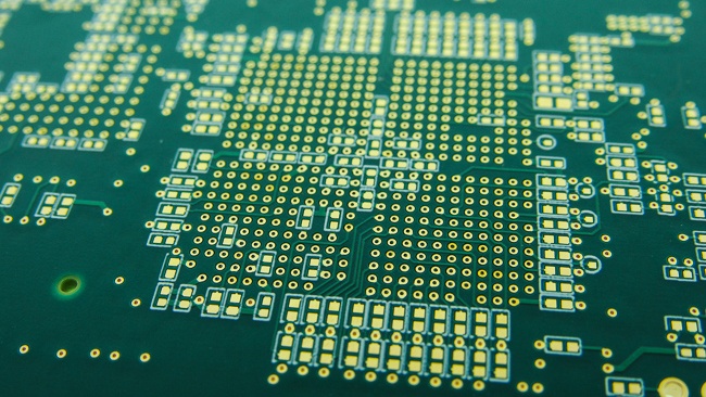
Printed Circuit Board Using HDI Technology
Mechanical Drilling Vias
It is possible at times, if you only need to connect the external layer to a single layer below, to mechanically drill the vias down to about .006” diameter after all lamination is complete. This method will not add too much to the cost, but it is subject to some fairly strict limitations.
These limitations arise from the difficulty the fabricator will experience in plating the holes reliably unless the drill diameters are large enough in relation to their depth to allow for adequate plating solution flow. If the aspect ratio of diameter to depth is not generous enough, the solution cannot flow through the hole as it can when the hole extends through all layers, so air can become trapped inside the hole. The air blocks the solution from coating the inner and bottom surfaces of the hole.
The result is a void, and either an unreliable interconnection to the internal layer, or none at all. The deeper the hole is in relation to its diameter, the more pronounced this difficulty becomes. On smaller packages, the need for a pad large enough to support a .006” or .008” via can be a limiting factor as well. Good planning and solid process controls are necessary for success.
Laser Drilling Microvias
It is also possible at times to use a similar set of steps using laser drilled microvias. The main difference here is one of scale. The holes are smaller (commonly .003” to .004”) so in order to maintain the aspect ratio, the dielectric thickness must be reduced. The ideal aspect ratio for microvias is generally about 1:1. Dielectrics this thin often create secondary design challenges such as difficulty creating impedance-controlled signal traces wide enough to be processed while still meeting the correct impedance value.
Unrealistically thin traces may be omitted from the external layers and connected instead through the via to one or more internal layers where there may be more flexibility in balancing trace width and dielectric thickness to meet the target impedance. Fabricators capable of forming laser microvias must invest in costly equipment; processing the resulting holes is somewhat different as well. The special equipment and handling adds cost beyond the similar mechanical blind drilling process.
Blind Mechanical Drilling
Some blind mechanical drilling can also be done when the material is still in its core form (before any lamination) or certain groups of layers can be laminated together into substructures before drilling. The vias are initially drilled all the way through from the top to the bottom of the core or substructure, then plated normally before going to another lamination stage.
The interconnection quality using this method is excellent because the plating solution flows freely though the temporarily open hole. The holes can then be filled before the substructure is laminated to the remaining layers.
The costs associated with this method begin to add up on account of the multiple lamination stages (at least one more than normal) plus the drilling, plating, filling, and image processing required for each sub. If the external layer pads need to be restored to their original intact condition for surface mount component mounting (Via-In-Pad) then such processing will add more cost.
Stacked Microvias and Multiple-Stage Sequential HDI Lamination
For boards of the highest density, it is often necessary to resort to the use of stacked microvias and multiple-stage sequential HDI lamination. In this method, vias are formed one on top of the other by laser drilling multiple thin layers of dielectric material, then processing and laminating repeatedly until all of the necessary layers are interconnected.
This method offers obvious advantages for complex signal routing within very constrained areas, with the trade-off once again being the ever-mounting cost of processing. It is important when stacking that the vias which will end up buried after the extra lamination steps must first be filled to prevent voids and the number of extra lamination stages increases by however many layers must be interconnected.
Sequential lamination is often the only way to form the necessary interconnections, but the multiple laser cycles, plus the plating and filling required before the next layer can be added, makes it typically the most expensive method.
Summary
The point of the above information is not to discourage the design of HDI boards. On the contrary, as the need for miniaturization leads to the further development of ever-smaller product packages, the need for such PCBs will only increase. But understanding at least approximately how much your printed circuit board cost will increase with blind and buried vias is useful for project planning and may lead to consideration of less costly alternatives when such alternatives are possible.
We encourage designers to submit preliminary information for review in cases where multiple approaches are under consideration. We can often recommend the best, cost-effective, and most reliable solution for your project.
Key Takeaways
- Blind and buried vias enable miniaturization but increase cost: High-density interconnect (HDI) PCBs using blind vias are essential for compact designs but often require multiple drilling and lamination cycles that significantly add to manufacturing costs.
- Mechanical blind drilling is limited by aspect ratio and plating challenges: While relatively inexpensive, mechanical blind vias are only reliable when the hole depth and diameter maintain a favorable aspect ratio; otherwise, plating quality suffers.
- Laser-drilled microvias offer precision for HDI but demand special materials and processes: Microvias allow for smaller vias and denser routing but require thin dielectrics and expensive equipment, making this method costlier than standard drilling.
- Sequential lamination with stacked microvias is the most expensive option: Boards requiring the most compact routing often use multiple rounds of laser drilling and lamination, which offers maximum design flexibility at the highest cost.
- Early collaboration with your fabricator can reduce unnecessary expense: Sharing preliminary design details enables manufacturers to suggest more cost-effective alternatives to complex HDI structures where possible, improving reliability and reducing overall PCB cost.


