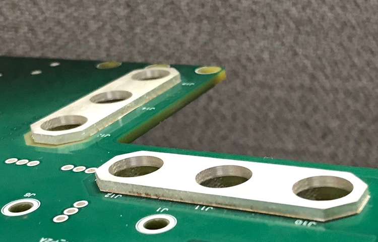
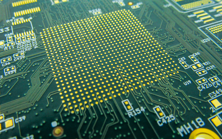
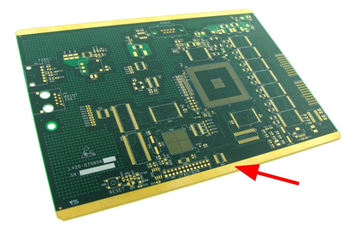
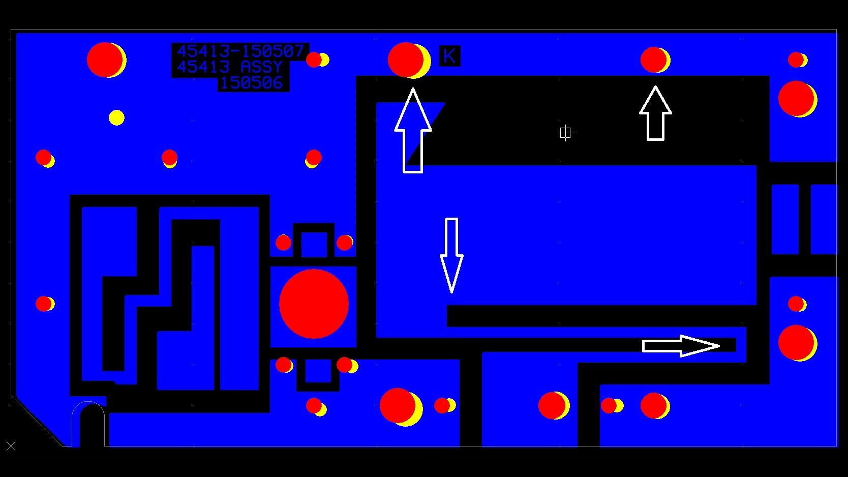
Designing a PCB with extreme copper plating requires planning and careful consideration of several factors that do not come up during the design of a standard, light copper board. Many fabricators avoid heavy and extreme copper circuit board orders entirely because of the unusual manufacturing challenges and non-standard processes associated with these product types.
Read MoreAl Wright

Recent Posts
When you are designing a printed circuit board (PCB), your customer or boss does not typically hand you a blank check. You may occasionally be fortunate enough to have a customer with deep pockets, but most products are very cost-sensitive, and your board design will need to come in at or below budget. This post will go over some of the things you can do to achieve a cost-effective design. Its focus will be limited to a handful of higher-end design options.
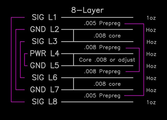
Read MoreAs somebody whose job it is to analyze several multilayer PCB designs per week, I find it surprising whenever I receive a data package that does not include a defined lamination stack-up. The way that the layers are constructed can affect the PCBs performance, so these packages feel like they are missing a potentially important piece of information.
Read MoreThere was a time when the PCB manufacturing industry included a fair number of bucket shops, so called because much of their processing was done in small portable tubs filled with etchants, solvents, and other mysterious solutions. They cranked out very basic, low-cost, low-complexity PCBs, using equipment and methods that were questionable at best. Their business and environmental practices were often similarly questionable.
Read MoreDesign for Manufacturing (DFM) is critical to the success of your PCB order. Features that make your circuit board difficult to build add cost to your product and can increase the scrap rate. If you have designed a PCB that is more complex than usual, it is useful to submit files to your fabricator for review before placing your order so you will have some time to address any issues that might delay production.
Read MoreAt the conclusion of our recent webinar – Match Your High-Tech PCB Design To Your Supplies Capabilities – we had a number of questions for our presenter, PCB Field Applications Engineer Al Wright. We decided to compile these into a readable format on our blog.
Read MoreOrdinarily you may not want your PCB (printed circuit board) manufacturer to adjust your data files, but there are occasions when that may be the easiest way to achieve a particular result. For instance, you may need to have some, but not all, vias of a particular size plugged so that the assembly solder will not wick through to the other side of the board. Or perhaps a few trace pairs need to run at a specified impedance, while the impedance for all the other traces of the same width is non-critical.
Read MoreThe design of a multi-layer PCB (printed circuit boards) can be very complicated. The fact that a design even needs to use more than two layers implies that the required number of circuits will not fit onto just a top and a bottom surface. Even in cases where the circuitry does fit onto two external layers with no problem, the PCB designer may decide to add power and ground planes internally in order to correct a performance shortcoming.
Read MoreOwing to the prevalence of complex processors, USB devices, and antennas printed directly onto the board surface, more and more PCB designs now require impedance control and testing than ever before. In response to the increased demand, circuit board manufacturers have invested in sophisticated modeling software and testing units, so they are equipped to meet the requirements.
Read MorePrinted circuit boards (PCBs) have become an integral part of everyday modern life, both at work and at home. PCBs were at one time found primarily where you would have expected them to reside inside computers, calculators, televisions, and other such obviously electronic devices, but now they present nearly everywhere.
Read More


