


Printed circuit boards (PCBs) have become an integral part of everyday modern life, both at work and at home. PCBs were at one time found primarily where you would have expected them to reside inside computers, calculators, televisions, and other such obviously electronic devices, but now they present nearly everywhere.
Military, industrial, automotive, aerospace, medical, and commercial applications are almost limitless, as are the different physical configurations that are available. What follows is a look at some of the expanding range of applications where PCBs make our modern lifestyle possible.
A Brief History of the PCB
Printed circuits have been available for many decades, but the variant we recognize today really began to replace older point-to-point, hand-wired electronics starting in the 1960s, not long after the formation of the IPC in 1957. Around that time, processing methods became more standardized, and specialized materials became widely available.
The invention of the transistor (which replaced the bulky, hot-running vacuum tube) opened new possibilities for consumer electronics on the civilian side, while at the same time the Cold War and the Space Race were creating demand for cutting edge electronic devices tailored for military and aerospace use. Suddenly, everybody needed PCBs.

Earlier circuit boards had been produced either by additive methods (adding conductive materials to non-conductive surfaces) or by subtractive methods (removing some of the conductive material to form a unique circuit pattern on the non-conductive substrate.) Eventually, manufacturers realized that the ideal method was to combine subtractive with additive processing, to take advantage of the benefits of each. Suppliers developed copper clad insulating materials which could be produced by printing a photographic image of the particular circuit onto a base copper foil, then removing the copper wherever it was not needed. After that essentially subtractive step, various additive steps such as copper plating, surface metalization, and ink application, would produce a board that was reliable and repeatable.
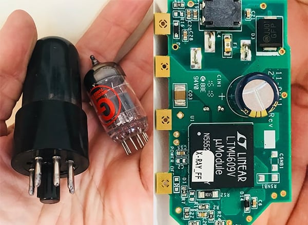
This PCB is nowhere near state of the art but compare it to the vacuum tube technology of yesterday.
Over time, these basic steps were further refined. This refinement has led to ever-increasing sophistication of the finished product, to the point where today’s boards are capable of supporting processors that are more powerful than anything imagined by the original PCB industry pioneers. What follows is a look at how emerging PCB applications are driving design trends.
Trends and Drivers: Smaller PCBs
The most wide-ranging trend is, as it has been for a long time, the relentless march of miniaturization. Components that end up being mounted onto PCBs are becoming so small, dense, and powerful that board designers and fabricators often find themselves struggling to come up with manufacturing design rules that will result in a functional unit. A new generation of tiny medical devices, wearable electronics, and ubiquitous smart devices has driven miniaturization beyond limits previously envisioned, as more and more tasks are controlled remotely by devices which must remain easy to carry while offering efficient use of ever-shrinking power sources. Smaller, lightweight circuit boards are the order of the day.
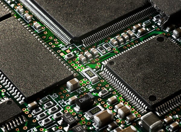
Example of printed circuit board assembly with miniaturized components.
In order to meet these requirements, components such as micro-BGAs use previously unheard-of pin-to-pin spacing and pad size, although their small land areas often make it impossible to route signal traces on anything other than the outermost row of pads on the external layers. The solution to this is to place blind laser microvias within the pads themselves, and to use sequential lamination (build up of the Z-axis a layer at a time) so that the necessary connections can fan out from the internal layers instead. While the largest and most sophisticated PCB suppliers have been dealing with these issues and fabrication techniques for years as a specialty, smaller suppliers are finding it necessary, given the increasing demand, to reinvest in new equipment required to produce this sort of work.
The increasing emphasis on miniaturization has also led to a marked increase in the use of mechanical solutions to electrical problems. For example, the problem of via stub length on high-speed designs can be mitigated by substituting blind microvias for through vias. Whereas a through via might often be drilled several layers past the highest numbered layer to which it is actually required to form an electrical connection (causing the signal to travel a greater distance than necessary) a blind via terminates at the same Z-axis depth as the last layer to which it connects. This reduced depth eliminates extra travel down the plated barrel of the via. The signal follows its true path, absent any extra distance that could adversely affect the critical timing.
A related technique is back drilling. Sometimes it makes sense to either avoid or minimize the number of sequential laminations, and to instead drill some or all vias as temporary through holes, coming back later with a secondary controlled depth drilling operation that removes the plating from the unused length of the hole wall. Back drilling is especially useful when the design has reached its maximum number of sequential laminations, but some additional interconnections are still necessary. The use of blind vias and back drilling are becoming more common as physically smaller and electrically faster boards use higher layer counts and denser circuitry.
While surface mounted processors and other devices are becoming ever smaller so that they can fit onto the external layers for assembly, some discrete components are disappearing from external surfaces altogether, being placed instead onto internal layers. This is especially prevalent with resistors, which in many high-density designs are now laminated onto various internal layers using specialized materials, making possible recovery of significant areas of the external surfaces. The recovered area then becomes available for placement of additional components, or the circuit board footprint can simply become smaller – the decision coming down to whichever design consideration is more critical. As an added benefit, aside from enabling the production of physically smaller PCBs, embedded components often enhance the electrical and performance of high-speed circuits, by shortening circuit paths.
Trends and Drivers: Larger PCBs
Moving towards the opposite end of the size and density spectrum, high-power boards are increasingly common, although they are hardly new. Technologies driving designers towards high power PCBs include the increasingly popular electric vehicles that often go unnoticed but are everywhere. When one thinks of these vehicles, it’s plug-in cars that come most readily to mind, but EV technology is established and growing in many other settings that might not be as obvious, until you start to look for them.
Consider your last trip to an airport, where EV’s handle many ground support duties, such as refueling, baggage hauling, and towing, plus delivery and removal services before and after flights. There is likely to be one or more heavy duty PCB inside most such vehicles. These circuit boards are often thicker than normal and are characterized by wide traces of heavier than normal copper weight; the components are primarily heavy duty as well. Designers who cater to this market segment aren’t looking to miniaturize. Rather, their priority is highly reliable performance in a demanding physical environment.
Heavy duty PCBs are also present in equipment you might take for granted, such as solar panels and lighting fixtures. Boards for these applications have their own unique combinations of requirements. The increasing popularity of LED lighting, for example, has led to an increase in demand for aluminum-backed PCBs. A major driver here is the replacement of fluorescent tubes with highly efficient LED arrays.
Circuit boards designed for this purpose are often simple but must be built on thermally conductive materials with aluminum backing which helps to disperse heat. One peculiarity of these boards is their length, which often exceeds the size range of traditional PCB equipment, so as designers create these larger boards, some manufacturers have responded by setting up lines optimized for production of what would previously have been considered oversized product.

Summary: Get Ready
The printed circuit board design trends above do not necessarily represent brand new technologies. Rather, they show that as the product mix changes in response to shifting demand, PCB designers and manufacturers need to adapt in order to position themselves to take advantage of the growth areas within the electronics market. Those who do not prepare may find themselves left behind at the next bend in the road, which would be regrettable, since falling behind now could lead to unfortunate missed opportunities in the near future.
With so many emerging applications in robotics, mobile devices, artificial intelligence, and the Internet of Things (IoT), individuals and companies who do manage to change on the fly should have no trouble finding ways to remain busy over the next several years.
Key Takeaways
- Miniaturization remains the leading driver: Consumer, medical, and wearable devices push designers toward ever-smaller, lighter PCBs with dense components, micro-BGAs, blind microvias, and sequential lamination.
- Mechanical techniques support high-speed performance: Methods like blind vias and back drilling reduce via stub length, improving signal integrity and timing in high-speed, high-density boards.
- Embedded components free surface space: Resistors and other discrete parts are increasingly laminated into internal layers, allowing smaller footprints or more surface area for additional components.
- High-power applications drive larger PCBs: Electric vehicles, solar equipment, and LED lighting require thick boards with heavy copper, aluminum backing, and oversized formats to handle high current and thermal demands.
- Adaptability ensures competitiveness: PCB suppliers that invest in new equipment and align with growth markets like robotics, IoT, and AI will remain strong, while those slow to adapt risk losing opportunities.


