


When you are designing a printed circuit board (PCB), your customer or boss does not typically hand you a blank check. You may occasionally be fortunate enough to have a customer with deep pockets, but most products are very cost-sensitive, and your board design will need to come in at or below budget. This post will go over some of the things you can do to achieve a cost-effective design. Its focus will be limited to a handful of higher-end design options.
For more comprehensive information on the topic of cost control in PCB design, this installment will conclude with a series of links. These links will point towards several previous installments that are also relevant.

PCB Cost Not Solely Based On Complexity
The most important point is that the cost of your circuit board does not depend solely upon its overall complexity. In many cases, a single process, tolerance, or feature may turn what is an otherwise unremarkable board into a low-yielding one that may be met with either requests for deviation – or outright no-bids – when you distribute it to potential manufacturers for a quote.
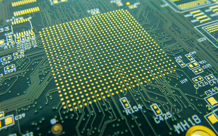
Example of printed circuit board BGA with trace/space requirements.
Low-End Technologies PCB Designs
At the low-end of the technological spectrum, mechanical callouts are a source for concern. For example, we occasionally see double-sided PCBs which require material thicknesses that are not commonly available, or which come with unrealistic thickness tolerances.
Our first strategy is always to suggest a standard thickness that is easy and cheap to procure. This simple suggestion clears things up painlessly in 75% of the situations, many of which result from the PCB designer’s unfamiliarity with what is considered standard. In other cases, though, the circuit board might have been an afterthought within a larger project, designed to fit inside of an enclosure that has a certain amount of space inside. If it is a multilayer printed circuit board, then the fabricator can often mix and match core and prepreg material sheets to laminate to the correct overall thickness.
With 2-layer work, however, this adds cost. It also prevents the PCB fabricator from certifying the resulting material to meet UL standards, because the fabricator is not a UL-listed manufacturer for core materials. It is best, then, to design to standard material thicknesses with standard tolerances.
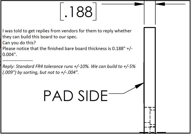
This +/- 0.004” material tolerance is far too tight for 0.188” thickness, although the PCB is otherwise simple.
Mid-Level Technologies PCB Designs
On mid-level designs, a single micro BGA (or similar high-density device) can drive up your costs. Even if the rest of the PCB follows very standard design rules, the fabricator must adjust the process to accommodate the one high-end feature. It essentially becomes the “worst-case” element of the design, introducing the need for special handling, special materials, or both.
While the added cost may not be as high as it would be for a design that incorporated a host of difficult features, the price will nevertheless be significantly higher than standard. Sometimes that smallest feature is an absolute necessity, either for proper function, or for reducing the PCB footprint to fit the available space. In those cases, the extra cost is worthwhile. Nevertheless, it is worth at least considering a different component with more forgiving characteristics, before settling on the smallest available processor.
High-Level Technologies PCB Designs
Many new PCB designs absolutely require high-end materials and processing, making it impossible to produce them inexpensively. High-frequency laminates, multiple cycles of high-density interconnect (HDI) with sequential lamination, and features such as cavity formation and back drilling, all contribute to the high cost of truly sophisticated designs. Embedded components and laser direct imaging (LDI) are two technologies that make it possible to design ever-smaller PCBs.
In the eternal quest for greater and greater miniaturization, some passive components that began long ago as through-hole types, before being shrunk to ever-smaller surface-mounted versions, are now moving to internal layers, where they are formed by imaging from a sheet. Embedded components require special materials that can be laminated between the other layers of the board, adding functionality while removing clutter from the top and bottom surfaces. Attractive as this sounds, not every fabricator offers embedded component processing, and those that do will charge premium prices. As with any other high-end design feature, it is useful to know that such technology exists. It is also important not to design-in the added cost, except in cases where there is no less costly alternative.
For extremely tight HDI boards, where the trace/space requirements fall beyond the limits that can be reproduced with traditional film processing, laser direct imaging has become increasingly common. The main advantage of LDI is that it can produce smaller, tighter, and more consistent feature sizes than traditional film-to-film exposure. The downside, beyond the investment in equipment, is that it requires significantly more time per panel than a photo exposure. Whereas a photo exposure takes seconds, LDI requires the laser to move all around the design, forming one feature after another, in much the same manner as a CNC routing machine, or a flying-probe continuity tester. Throughput has gotten much better since LDI was first introduced, but it remains a premium process, offered at premium pricing. If you can lay out your PCB with slightly more forgiving design rules, LDI will not be necessary.
Summary
The point is the same for all elements of your PCB design: try to exhaust the possibilities of existing, lower-cost technologies before moving forward with more cutting-edge features. As mentioned, some applications demand a state-of-the-art approach in order to meet a design requirement, and the equipment and processes needed to bring such designs to life do exist. Still, it pays to review each element of your design to be sure that you really need the more complex features that are likely to add cost, and to eliminate those that are not necessary. The rewards for teasing-out needless complexity are lower cost, and more predictable manufacturing.
* Four related blog posts listed for further reading:
- Controlling PCB Costs: Part 1
- Controlling PCB Costs: Part 2
- What is the Standard PCB Manufacturing Process?
- How to Manage PCB Design Cost Adders
Key Takeaways
- Single design features can drive cost: Even a relatively simple board can become expensive if one process, tolerance, or feature requires special handling or reduces yield.
- Standard materials and tolerances lower expenses: Designing with commonly available material thicknesses and tolerances avoids unnecessary costs and certification issues, especially on lower-layer count boards.
- High-density components increase complexity: A single micro-BGA or other fine-pitch device can raise manufacturing costs by forcing tighter process controls, even if the rest of the design is standard.
- Advanced processes come at a premium: Features like HDI with sequential lamination, embedded components, cavity formation, or LDI add significant cost and should only be used when absolutely necessary.
- Exhaust lower-cost options first: Reviewing each design element to determine if standard technologies will suffice and help reduce cost while ensuring more predictable manufacturing results.


