


Avoiding Expensive PCB Materials & Processes
Printed circuit boards are only one component of an entire assembly designed to meet the best cost-to-performance ratio possible. The finished product into which the PCB is installed must meet a price point that compares favorably against competing products, so the lower the expenses, the more money your product returns. In order to make the best choices during the design cycle, it is important to first understand what drives the primary costs.
Once you understand what components add to the overall printed circuit board cost, you can start designing your PCB to perform to your needs while keeping your price manageable. In part one of a two-part blog post, we detail some common cost drivers with suggestions on how to avoid incurring them within your design.

PCB Laminate Selection: Find The Right Balance
Selecting the appropriate printed circuit board laminate is just the first step, with many additional elements to consider. Begin by selecting a material which meets your requirements for electrical and thermal performance. For instance, if you have controlled impedance requirements, then you will need to consider Dk and Loss Tangent specifications. If you will be employing multiple assembly cycles (2-sided SMT assembly, for example) then pay attention to thermal performance, such as Tg, Td, and CTE. At all times keep in mind the surface finish you will be using. Higher soldering temperatures are required for lead-free finishes will put greater thermal demands on your material.
Your goal should be to meet or exceed all performance requirements without paying extra for unnecessary components. If your design is a 4-layer, power/ground PCB with SMT components on only one side, you may not need to give as much weight to the CTE as you would for a 12-layer PCB with 2 sides SMT, BGAs, etc.
Whenever possible, specify your material to industry standards. The best way to proceed is to familiarize yourself with the materials as defined in IPC4101C and to call out the laminate by the “slash number” for the set of specifications that will meet your needs. As a starting point, all fabricators will stock materials that meet 4101C/21, /24, /26, and to an increasing extent, /126.
One final word: Be sure not to go overboard trying to save money. Skimping on material at the front end can cause costly failures at assembly, or later in the process, where the added value will far exceed the cost of using what would have been the appropriate laminate for the bare circuit board.
Avoid Excessive Blind & Buried Vias
Printed circuit boards are getting smaller and smaller, and it is necessary to use every little bit of space to form interconnections. This trend drives an increase in the need for blind and buried via drilling, which in turn requires sequential lamination (meaning that the PCB must undergo multiple lamination cycles so that each set of drilled holes can be drilled, plated, and processed before all of the sub-laminations are put together.) The combination of blind and buried drilling with multiple lamination cycles is called High Density Interconnect (HDI) processing.
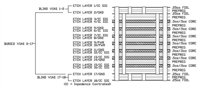
Minimize the number of extra drill and lamination cycles whenever possible. Try not to exceed 4 drill cycles (2x blind, 1x buried, 1x through all.) Here is a typical cross-section for a 18-layer PCB with a total of 4 drill cycles and 2 laminations. This requires only 1 more lamination step than a standard multilayer, and the drilling is balanced about the centerline.
HDI processing is practically routine when it is well-designed, but it remains expensive, and a poorly-planned HDI design can be difficult or even impossible to produce. We once received an RFQ submission for a very simple, low-density 10-layer PCB with 7 different drill cycles. That printed circuit board was literally impossible to manufacture, and our only choice initially was to no-bid it. We did provide some suggestions, which helped the customer to re-think his design, and to come up with something more workable.
When designing an HDI PCB, try to limit blind drilling to the top and bottom layer, connecting to the immediately adjacent layers, while limiting buried vias to a single pass which connects the two outermost internal layers. For example, a 12-layer with blind vias from 1-2 and 12-11, and buried vias from 2-11, only adds one extra lamination and HDI processing cycle. While this will not cover every eventuality, it is an ideal configuration for manufacturing.
If you initially find yourself needing a large number of blind and buried layer interconnections, look for ways to simplify. The fewer lamination cycles are necessary, the less your PCB will cost. The customer above, who started out with 7 drill files, eventually managed to make all of his interconnections using only through vias, without resorting to any HDI processing at all.
Inefficient Machining
When drilling or routing circuit boards, PCB fabricators typically improve throughput by stacking the material so that multiple sheets may be processed simultaneously. For example, 0.062” thick PCBs are most commonly drilled in a 3-high stack, with even 4-high possible. Stack height is typically determined by the diameter of the smallest drilled hole, which has been shrinking steadily because of the ever-smaller via diameters required as PCBs become smaller and smaller. Use of materials thicker than 0.062” also affects stack height.
CNC Machines typically employ three or more spindles for drilling and routing. The more panels for fabricator can stack under each spindle, the more economical these processes become.
With miniaturization driving PCB designs towards higher density, it is pointless to recommend that all vias be specified at, say, 0.028” diameter, so they can be drilled in a 3-high stack. Nonetheless, if it is possible to use vias that are 0.015” or 0.018” diameter, instead of 0.010”, and if doing so will not either create spacing problems, or drive you to a higher layer count, then consider using the larger size. Doing so will allow for 2-high drilling, which will cut drilling time for your order in half compared to a design that uses 0.010” or 0.008” vias.
The same goes for routing. Routing cost drivers include small slot widths, small minimum inside corner radii, and small channel size on routed sub-panels. Slot or channel widths below 0.062”, and inside radii below 0.031”, will reduce your fabricator’s stack height from three to two. Below 0.047” width and 0.023” radius, the stack height drops again, to one. Avoid cuts that require small-diameter routing burrs whenever possible, and consider drilling relief holes at inside corner locations, in place of small radii, when a flush fit is required. Routing is one of the final steps before shipping; an overly long cycle time draws a lot of attention and adds cost to your order.

Summary
Lamination, drilling, and routing are all bottleneck departments in the circuit board production cycle that contribute to the overall cost. Awareness of PCB cost drivers within these processes will help you to make informed decisions about which design features are advantageous, while eliminating those which are not. Learning to implement these best practices will result in a reliable product at the best possible price.
Learn more ways to save in our Controlling PCB Costs: Part 2 post!
Key Takeaways
- Laminate selection impacts cost and reliability: Choose laminates that meet thermal and electrical needs (Tg, Td, CTE, impedance) without over-specifying materials that add unnecessary expense.
- HDI designs increase costs with each drill and lamination cycle: Keep blind vias limited to outer layers and buried vias to a single pass; excessive drill cycles can make designs difficult or impossible to manufacture.
- Efficient drilling reduces expenses: Via sizes influence stack height; using slightly larger vias (e.g., 0.015” instead of 0.010”) can double throughput by allowing multiple-panel drilling.
- Routing tolerances affect stack height and cost: Very small slots, channels, and corner radii force thinner stacks, increasing cycle time and manufacturing cost.
- Cost savings require balance: Avoid over-engineering features that add lamination, drilling, or routing complexity; focus on manufacturable designs that meet performance needs while controlling overall PCB cost.


