


Printed circuit board (PCB) designers often find themselves at odds with their purchasing and marketing departments after a design goes out for bids and comes back with a larger than expected price tag. Once the source of the high cost is identified, the questions fly, the fingers point, and the nerves fray.
- Why didn’t somebody see this coming?
- What happened that made the project so costly, when it seemed so straightforward?
- How does this affect our time to market?
- How do we recover?
Sometimes high cost originates at the project planning stage, either necessary research goes undone, or the right people are not consulted. For example, if a connector can only function with a PCB of non-standard thickness, then the PCB will require custom-manufactured base material. Suddenly, that seemingly simple 2-layer PCB will cost far more than it would have cost had the connector been designed around commonly available PCB materials instead. Now, however, there is no turning back, so a PCB which had been an afterthought to the connector design team turns out to be a major cost driver for the project.

Other times, the desire to use a single non-standard feature on the board itself – a state of the art processor for instance, or an unusual surface finish may force the PCB designer to create one small area which is more difficult to produce than the rest of the board. Although, that area may seem insignificant, its presence may nevertheless force the fabricator to add several process steps and to apply tighter process controls. These drive up the cost of what might otherwise have been a generic and inexpensive board.
It is best to get everybody together at the start of a project, to be sure that these scenarios do not play out. It also pays to “know what you don’t know.” Familiarize yourself with standard materials and practices before plunging ahead. If you have a design feature that you suspect may be out of the ordinary, talk to the people who will be manufacturing your product. It is in their interest to help you navigate around any potential problems before they find them on their own production floor. For your part, make an effort to understand which of your design choices is likely to add cost, and then avoid those choices whenever it’s possible to do so.
Project Planning
Your best strategy for avoiding unwelcome surprises is to be aware of what constitutes standard processing. First, involve enough of the right people at your project planning stage. To identify the right people, have a kickoff meeting between all the parties - who will be involved in the design, manufacturing, or marketing of the product. The entire group does not need to remain intact throughout and it is probably better to cut back to a smaller group once the initial discussions have taken place. But if everybody at least gets a look at the plan and is invited to supply constructive comments, it should be possible to discover major flaws early in the cycle and to develop alternate approaches wherever necessary. Sometimes just one insightful comment or one simple question may make the difference between a project that rolls along smoothly and one that grinds to a halt.
It is also important to understand what is driving the most complex aspects of your design and to decide whether or not you may be able to live without some or all of them. The most spectacular cost overruns and the worst production yields are often the result of a poorly-chosen component or a PCB designed as an afterthought to fit an enclosure that does not allow for a reasonably standard PCB size or shape to fit within it.
A component footprint that is so dense as to require tiny pads, spaces, and circuitry may complicate production by requiring extra steps such as sequential lamination and laser drilling. A connector designed to accept a non-standard board thickness to make a secure connection could necessitate a custom PCB material order. An enclosure with an unusual height constraint or one which includes a very complex outline better suited to sheet metal machining or plastic molding may require that the PCB outline adhere to tighter than normal tolerances and extra machining steps. Again, if you encourage all involved parties to bring their specific areas of expertise early on, it may be possible to identify a simpler way to accomplish the same design goals.
Now it is time to address some common cost adders.
Cost Adder: Non-Standard Plating
We will confine this section to copper plating. For most PCBs, the word “plating” refers to the electroplated copper applied to the surface of the circuitry and in the barrels of the holes.
Most commonly, internal layers of multilayer PCBs do not receive added copper. Instead, the internal circuit patterns are simple printed with a film resist, exposed, developed, and etched. However, external layers receive additional plating which is applied to the exposed surface circuitry at the same time that the plated through hole interconnections are formed.
Most fabrication notes are straightforward when it comes to copper plating. There should be a note describing the average thickness of the copper in the holes (.0008” average, .0007” minimum for Class II, .0010” average, .0008” minimum for Class III). There should also be a callout for the weight of the copper circuitry. Usually, the external copper weight is interpreted as the final after-plate copper weight, the total of the base foil plus the added plating.
Copper that needs to be thicker than Class II or Class III will require special handling at extra cost. One reason is that automated plating lines may use fixed settings that will need to be modified to do your special process. Since automated lines often run panels from several different part numbers at once, changing settings may require the removal of all other panels from the line while yours runs through.
Even with manual plating more plating requires more time in the tank. The additional copper that is being applied is expensive as well. If a panel is plated too long the copper my end up “mushrooming” over the photoresist which defines the circuit pattern. If this happens, the copper which has come up over the resist boundary will encapsulate the resist making it very difficult to remove and potentially scrapping the job.
To avoid incurring extra costs related to copper plating it’s best to stick with standard copper plating in the holes (Class II or Class III) which will yield external copper pattern plating around .0010”-.0014” over the base foil. Other copper options are often available (including heavier plating, selective heavy plating, etc.) but these come at additional cost and will in most cases be subject to modified design rules and a full fabrication DFM review.
Cost Adders: Via-In-Pad, HDI, Sequential Lamination
If your design is very dense and uses very tight-pitch components it may be that you will need to use SMT and/or BGA pads as via drilling locations which will then be filled, planarized, and plated over so they can be used for component soldering. This type of processing is increasingly common, but it does add significantly to your cost.
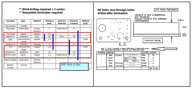
Example of PCB Documentation with Sequential Lamination
The simplest form of via-in-pad processing involves drilling through vias from top to bottom. These are drilled before the rest of the plated through holes so they can undergo extra steps that will result in a filled, capped via. After drilling they are plated, filled with epoxy, and then planarized in a polishing step that brings the epoxy flush to the copper surface. After the remaining plated through holes are drilled the board proceeds more or less normally to completion. This simple via-in-pad processing adds cost, but it is not as extreme as full HDI (high density interconnect) processing.
HDI involves multiple drilling, plating, and filling steps. A sub-structure of internal layers may be drilled through. For this example, we will use layers 3 to 6 of an 8-layer PCB. These are processed much the same way as a fully-laminated multilayer with plating, filling, planarization, and imaging all being completed. Additional layers are then laminated onto the internal sub-structure. These are drilled usually by a controlled-depth process that connects only the outermost layers with their adjacent layers (in this case, drilling would be L2-L3, and L7-L6). These holes may be mechanical, but they are more often laser-formed because of their extremely small diameter (.003”-.004”). When these holes have been treated the top and bottom layers are laminated to the sub-structure. Additional blind drilling occurs followed eventually by through-hole drilling and then the remaining standard process steps.
An HDI board passes through many more steps than a normal board or even a board with standard through-hole VIPPO processing and it may go through those extra steps 3 or 4 times before the entire stack is laminated. If you need it done, then you need it done. Do keep in mind that the cost of performing certain steps many times, coupled with the fabricator’s investment in specialized equipment, will add significantly to the price of the finished PCB. You may find in some instances that adding more layers will reduce the signal density enough for you to eliminate some of the HDI interconnections. The result could be a less expensive board that is somewhat faster and easier to process.
Cost Adders: Drilling & Routing
Almost all PCBs require at least some drilling. Routing is still a common removal method too, although, boards may also be cut out by v-scoring or even punching.
While drilling is a standard process and would therefore not seem to add cost, limits exist in the drilling process and can lead to inefficiencies that show up as money. Most have to do with how many panels can be drilled in a single pass on the CNC machine.
Example of PCB with Small Router Channel
Fabricators typically want to drill 2 or 3 panels at a time on each head of their CNC machines. Panels are stacked and pinned together, loaded onto the machine, and all diameters drilled in order during one cycle. If a single table load of boards requires 20-minutes to complete, it is obviously advantageous to drill as many panels as possible at the same time. Thirty years ago, when most boards used through-hole components and vias were large and relatively few, almost all orders could be pinned 3-high.
Eventually though, a higher percentage of components were smaller surface-mounted types. These had a greater pin density so to provide the necessary number of interconnections to service the density vias became smaller and more numerous. A typical 2,000-hit table load became a 10,000-hit table load. At the same time, the drills themselves became much smaller with shorter flute lengths that made them more susceptible to breakage.
Since the short drill bits could not penetrate more than two panel thicknesses (at best) without either breaking or smearing the hole with debris, panel stacking became problematic. Most fabricators now have a cutoff for how small a bit they can use for 2-high versus 1-high. Generally, anything drilled at .012” or below is likely to require 1-high drilling so instead of a 4-spindle machine producing 16 completed panels of 2000 holes every twenty minutes as in the past, that same machine might be drilling just 4 panels of 20,000 holes every 40 minutes.
The industry has responded to the exponential increase in small vias by making air-bearing spindles standard ramping up both spindle and table speeds significantly and introducing super-efficient dedicated via drilling machines to keep up. Nevertheless, the difference between using a .014” via and a .008” might be the difference between 2-high and 1-high drilling. Even with the best and fastest equipment it is still possible to create a bottleneck in the drilling department that can show up as a factor in higher pricing for your PCB.
CNC routing is usually routine. If the program simply cuts around the perimeter of the PCB or does a limited amount of travel during a tab-routing program for a multiple-PCB array, costs are standard. Routing only becomes more expensive if it requires tools that are either smaller than normal or need to travel farther than normal or both.
For example, a small PCB that will be supplied in an array with tabs to hold the boards in place during assembly may spend a long time on the machine because of the cumulative distance it needs to travel and because of the many times it will pause, lift, plunge, and resume along the way. As with HDI processing, if this is what you need, then this is what you need, but it may add cost. If the board also requires a small tool path (perhaps to form a tight inside corner radius or a slot) then the panel stack height will also be affected, and you will end up paying for the less efficient use of machine time.
Sometimes you can get around tab routing to some extent by eliminating the tabs and instead holding the boards into the panel by v-scored flats when they are available. This is a good strategy if you have a couple of 90-degree edges that can be scored in a straight line and if the edge is not critical to your PCB fitting into its enclosure. Saw blade V-scoring is so much faster than routing that even adding the extra operation will end up saving money compared to an inordinately long routing cycle.
PCB Manufacturing Explained: The V-Score & Jump Scoring Process
The rule of thumb is that any board which will require routing with a bit smaller than .062” will usually need to be routed less than 3 panels high. Small slots or small inside corners (less than .031”) require smaller tools and will drive the stack height down. Compounding the stack height problem, small-diameter bits need to run at slower table feed rates so the machine may be run twice as long with a small tool as it would need to run the same distance with a .093” or .100” tool.
One last item on this topic is controlled-depth routing. Sometimes features need to be milled out of the surface without cutting all the way through the PCB. Other times a single-sided score is required and since this can’t be done on a normal scoring machine (which uses two circular saws facing one another) this will need to be done with a custom scribing bit and a special Z-axis setting. Milled features require a good deal of setup time to dial-in the correct depth before they run. The panels obviously cannot be stacked since the router is not passing all the way through even one PCB. When a PCB requires controlled-depth milling or single-sided v-cutting, it will spend a good deal of extra time tying up the CNC router and this will come at a cost.
To counter some of the inefficiencies associated with small tools you may wish to consider going to a thinner PCB.
Cost Adder: Poor Material Utilization
Aside from the use of exotic material types (which we will not cover here) the most significant cost adder of all is poor material utilization. The reason it is so important to design your board to high-yielding dimensions is that a poor-yielding design will compound every one of the adders described above and will cripple the fabricator’s throughput. If you have a board that already requires thicker than normal plating, small drills, and a long routing cycle, then you already have a problem. But if your fabricator can only fit two of them onto a standard sized sheet of laminate because your board is slightly too large to run 4-up, then you are costing yourself twice as much money on each board you purchase. It is therefore well worth reviewing your board size with your fabricator as early as possible in the design cycle to see if it’s possible to make improvements.
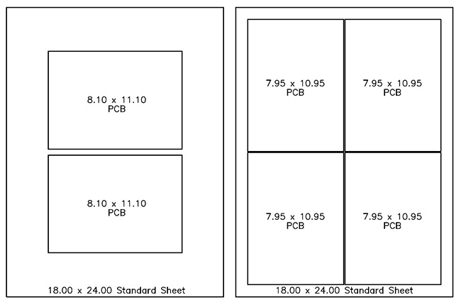
Poor PCB Material Space Utilization

There are of course several common PCB configurations which are designed to fit into existing racks or enclosures. The options for changing the dimensions of such boards are limited. But if you have a custom product and some flexibility it pays to find out whether your PCB will yield well before you route all of the circuitry and add all of your bells and whistles. While you are at it, find out what the impact will be if you then choose to receive the board in a multiple-PCB array or with temporary assembly rails added to one or more edges. Many times, either adding or trimming just a fraction of an inch from one dimension or the other will make all of the difference in the world to the final board cost.
Summary
The information above is not meant to discourage anybody from using features that will be critical to the success of their design. If you need a feature, then you should use it. Rather, the point is that if you understand which factors are likely to drive your costs up you will be better equipped to choose less costly alternatives wherever possible in order to bring your project in as inexpensively as possible. Using a slightly larger via size, trimming a tenth of an inch from the outer dimensions, or v-scoring instead of routing can all help to make your board cheaper and easier to produce.
Including the right team members during the initial project planning stage and asking questions of your fabricator as the project begins to take shape are helpful strategies for steering you clear of missteps that could drive up the price of your PCB. Your fabricator should always be glad to offer suggestions that will simplify production. Keep in mind that asking a question now will save time, trouble, and money later.
Key Takeaways
- Early collaboration prevents surprises: Bringing design, manufacturing, and marketing together at the start helps catch non-standard features or material requirements that can drive costs higher.
- Non-standard features add complexity: Unusual plating thicknesses, high-density interconnects, or non-standard finishes may require extra processing steps, tighter controls, and specialized equipment, all of which increase cost.
- Drilling and routing are major cost factors: Very small vias, dense hole patterns, or long/complex routing cycles reduce panel stack heights and slow down CNC operations, raising production costs.
- Material utilization is critical: Poor panel layout or board dimensions that yield inefficient use of laminate sheets can double per-board costs. Small adjustments to size or array configuration can dramatically improve yield.
- Know what adds cost and when to avoid it: If a design truly needs advanced features like HDI or sequential lamination, they should be used, but designers can save money by opting for slightly larger vias, standard plating classes, or v-scoring over complex routing when possible.


