



As material, freight, and labor costs continue to increase, printed circuit board (PCB) designers and buyers are under growing pressure to reduce manufacturing costs wherever practical. While material selection and board construction often receive the most attention, PCB array design can also have a significant impact on manufacturing efficiency and overall product cost.
Start with the Manufacturing Panel Size
When evaluating array efficiency, it is important to understand how much of a production panel is actually available for PCB placement.
The average panel size used in many production facilities is 18 x 24 inches. Although other panel sizes may be used, this remains one of the most common formats for production.

Not all of that panel area is available for product placement. Space is typically required along all four edges for tooling holes, coupons, pinning, and clamping during manufacturing. As a result, approximately 1 inch per side should be reserved for production processing, leaving about 16 x 22 inches of usable panel area for the PCB array.
Understanding this usable area provides a foundation for determining how efficiently a design can be panelized.
Why Panel Utilization Affects PCB Cost
The dimensions of the PCB, including any tabs or extended features, determine how many boards can fit on a production panel. Higher panel utilization generally means more parts produced from the same amount of material.
Increasing the number of boards per panel can reduce the material cost allocated to each unit while also reducing the number of panels required to complete a production order.
For this reason, panelization strategy should be considered early in the design process rather than after the PCB layout is complete.
Scored Arrays Can Increase Material Utilization
Consider a PCB measuring 6.5" x 8".
When the design allows the PCB edges to be scored rather than routed, boards can be placed directly adjacent to each other within the panel. In the example provided, six boards fit within the panel configuration, resulting in approximately 72% panel usage.
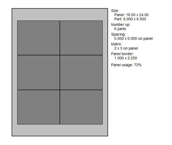
PCB Panel Array with Scored Edges
Because scoring allows tighter board placement, it can improve material utilization and reduce cost per unit when the PCB design and product requirements permit its use.
Routed Edges Reduce Available Panel Space
Some applications require PCB edges that are flat, smooth, and produced with a routed finish. In these situations, additional spacing must be maintained between boards to accommodate the routing process.
A minimum spacing of 0.1" is required between adjacent PCBs to allow the router to pass between boards without causing damage.
 PCB Panel Array with Routed Edges
Using the same PCB dimensions and orientation as the previous example, the number of boards that fit on the panel decreases from six to four. Panel utilization drops from 72% to 48%, representing a 33.3% decrease in parts per panel.
While routed edges may be necessary for certain designs, the reduction in panel utilization should be considered when evaluating overall manufacturing cost.
More Material Utilization Does Not Always Mean Lower Cost
A common approach to increasing panel utilization is rotating some circuit boards within the array to capture additional material area.
In the example shown, rotating two boards 90 degrees increases panel utilization by approximately 12%. At first glance, the higher utilization appears to provide a cost advantage.
 PCB Panel Array with Increased Usage
However, increased material utilization does not automatically result in lower manufacturing costs.
Rotating parts within an array can introduce additional tooling requirements, programming complexity, and plating considerations. In some cases, these changes can create manufacturing challenges that offset the expected savings. Increased scrap rates and production difficulties may ultimately eliminate any benefit gained from the higher material utilization.
Because of these tradeoffs, panel utilization should be evaluated alongside overall manufacturing efficiency rather than as an isolated metric.

Design PCB Arrays with Manufacturing Yield in Mind
For small PCB designs, a consistent array strategy generally provides the best opportunity for achieving favorable manufacturing yield.
When routed arrays are required, maintaining 0.1" spacing between boards and using 0.25" rails to support the array provides an established framework for production. Increasing board spacing or rail dimensions remains an option, but doing so also increases the amount of non-productive area within the panel.
The goal is to balance manufacturability, yield, and material utilization while minimizing unnecessary waste.
Summary
PCB array design can have a meaningful impact on manufacturing cost, material utilization, and production efficiency. Understanding usable panel space, evaluating scoring versus routing requirements, and carefully considering array orientation can help identify opportunities to reduce cost without creating unnecessary manufacturing challenges.
The most effective panelization strategies balance panel usage with manufacturability and yield rather than focusing solely on fitting the maximum number of boards onto a panel.
Key Takeaways
- Panel size is key to cost efficiency: Standard production panels are 18 x 24 inches, but with edge allowances, usable area is about 16 x 22 inches. Maximizing parts per panel directly reduces unit cost.
- Scoring improves panel utilization: Allowing PCBs to be scored instead of routed can fit more boards per panel, increasing usage percentage and lowering cost per unit.
- Routed edges reduce panel yield: Requiring routed edges forces spacing between boards, lowering material usage efficiency and raising per-board costs.
- Rotating circuit boards aren’t always cost-effective: While rotating parts may increase material usage, it can also add tooling complexity, plating challenges, and higher scrap rates, which sometimes outweigh the savings.
- Consistent array design improves manufacturing yield: Small parts benefit from arrays with standard spacing and rail dimensions, which balance manufacturability with material efficiency.