


Gold surface finishes serve different functions in printed circuits board (PCB) manufacturing, and selecting the right option depends on assembly requirements, durability needs, and overall cost objectives. Understanding the differences between ENIG, ENEPIG, hard gold, and flash gold helps designers choose the most appropriate finish for their application while balancing manufacturability, reliability, and lead time.
Understanding Gold Surface Finishes in PCB Manufacturing
Gold plating is widely used in PCB manufacturing, but not all gold finishes serve the same purpose. Different gold surface finishes are designed to support specific assembly methods, mechanical requirements, and reliability objectives.
Choosing the correct surface finish requires understanding how each process affects solderability, oxidation resistance, durability, shelf life, manufacturing complexity, and cost.
Gold as a Precious Commodity
Gold purity is commonly measured using the Karat (K) system.
Examples include:
- 24K gold: 100% pure gold
- 22K gold: 91.67% gold and 8.33% other metals
- 18K gold: 75% gold and 25% other metals
While these values are commonly associated with jewelry, PCB gold finishes differ significantly. For PCB applications, the gold used is 99.9% pure gold.
Because gold is an expensive material and largely becomes a waste product during assembly, selecting an appropriate finish is an important cost consideration during PCB design.

Gold Surface Finishes Used in PCB Manufacturing
Several gold-based surface finishes are available for printed circuit boards. Each offers distinct performance characteristics and is intended for specific manufacturing or end-use requirements.
Common options include:
- Electroless Nickel Immersion Gold (ENIG)
- Electroless Nickel Electroless Palladium Immersion Gold (ENEPIG)
- Hard gold for gold fingers and contact surfaces
- Flash electrolytic gold
The selection should be based on the application's assembly process, mechanical wear requirements, reliability goals, and budget.
ENIG Surface Finish
What Is ENIG?
Electroless Nickel Immersion Gold (ENIG) is one of the most commonly specified PCB surface finishes.
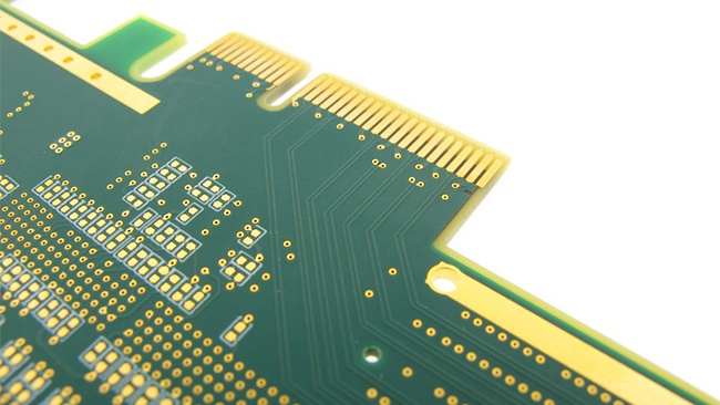
ENIG consists of a gold layer deposited over electroless nickel. The finish provides oxidation resistance while delivering an extremely flat surface that supports efficient assembly processing.

PCB Manufactured with ENIG Surface Finish
Benefits of ENIG
ENIG remains popular because it offers:
- Excellent flatness
- Good oxidation resistance
- Compatibility with SMT assembly
- Consistent processing characteristics
The gold layer is typically processed at 1–3 micro-inches, making it relatively easy to control during manufacturing.
Considerations for Increased Gold Thickness
In some cases, PCB designers request thicker gold deposits in the 4–8 micro-inch range. While this increases the amount of gold present on the PCB surface, it also introduces:
- Higher material costs
- Longer lead times
- Additional production processing requirements
- Reduced manufacturing throughput
- Commonly has assembly issues due to gold excess
According to IPC-4552 guidance, increasing the gold deposit may also compromise the underlying nickel layer, which serves a protective function within the finish structure.
ENEPIG Surface Finish
What Is ENEPIG?
Electroless Nickel Electroless Palladium Immersion Gold (ENEPIG) builds upon the ENIG structure by adding a palladium layer between the nickel and gold.
The palladium layer was introduced in part to address historical concerns associated with early ENIG implementations, including non-wetting and black pad issues.
Advantages of ENEPIG
ENEPIG offers several benefits, including:
- Improved wetting performance
- Enhanced shelf life
- Suitability for wire bonding applications
These advantages make ENEPIG a viable option for specialized PCB requirements where these characteristics are important.
Cost and Lead Time Tradeoffs
Despite its advantages, ENEPIG did not achieve the broad adoption many initially expected.
Factors contributing to this include:
- The high cost of palladium
- Additional processing requirements
- Dedicated manufacturing lines
- Extended production lead times
The process can increase costs by approximately 35%–60%, depending on production volume. Because of processing requirements, ENEPIG production is often scheduled only when sufficient volume exists to justify running the line increasing lead time in some cases by several weeks.
Gold Fingers and Hard Gold Plating
When Gold Fingers Are Used
Gold fingers are commonly used on PCB edge connections and contact surfaces that interface directly with mating connectors.
PCB Manufactured with Gold Fingers
Application requirements determine whether an immersion finish or a hard gold finish is appropriate.
For example:
- Circuit boards inserted once and left in service may utilize immersion surface finishes.
- Circuit boards that experience repeated insertion and removal benefit from hard gold plating.
Hard Gold for Mechanical Durability
Hard gold is designed for applications involving repeated mechanical contact.
Common examples include:
- Edge-card connectors
- Motherboard interfaces
- Membrane switch contacts
- Keypad contact areas
Gold plating thickness on keypad contact tabs is commonly specified at 30–50 (µin) micro-inches.
Hard gold is intended to withstand repeated use, including insertion, removal, and actuation cycles that may exceed 1,000 actuations.
Typical Hard Gold Thickness for PCB Edge Fingers
For PCB edge connectors, often referred to as gold fingers, the IPC standard does not define a single fixed gold thickness for every application. Requirements depend on the finish type and are covered primarily by IPC-4552 for ENIG, IPC-4556 for ENEPIG, and IPC-4554 for electroplated nickel/gold used on hard gold edge contacts and other wear surfaces.
For hard gold edge fingers, a common industry specification is 30 micro-inches of hard gold over 100–200 micro-inches of nickel. This is often used for standard commercial edge connector applications. For higher insertion-cycle or more demanding applications, 50 micro-inches of hard gold over 100–200 micro-inches of nickel may be specified.
Typical fabrication drawing callouts may include:
- 30 µin hard gold over 100–200 µin nickel
- 50 µin hard gold over 100–200 µin nickel for high insertion-cycle connectors
- Selective hard gold on edge fingers only
- Beveled edge, typically 20° or 30°, depending on the connector specification
The nickel layer provides the foundation and barrier layer beneath the hard gold, while the hard gold layer provides the wear resistance needed for repeated connector insertion and removal. Because thickness requirements can vary by connector design, insertion cycles, and end-use environment, the gold finger callout should be clearly defined on the fabrication drawing and confirmed with the PCB fabricator during design review.
Electrolytic Gold Plating Process
Hard gold is produced using an electroplating process, also referred to as electrolytic plating.
Unlike purely chemical deposition methods, electroplating uses an electrical charge to control the deposition process. Gold thickness can be adjusted by varying plating cycle time.
Standard hard gold processing typically produces thicknesses between:
- Hard gold thickness (minimum) = 0.000015 inches
- Hard gold thickness (maximum) = 0.000050 inches
Flash Electrolytic Gold
What Is Flash Gold?
Flash electrolytic gold is a thinner hard gold coating designed to provide selective durability while maintaining solderability.
Because the coating is substantially thinner than traditional hard gold, it remains compatible with SMT assembly processes.
Flash Gold Thickness
Flash gold deposits are approximately 10% of the thickness of standard hard tab gold.
Typical flash gold thickness ranges include:
- Flash gold thickness (minimum) = 0.0000015 inches
- Flash gold thickness (maximum) = 0.000003 inches
This combination of limited thickness and solderability makes flash gold useful in applications that require a thin electrolytic coating rather than a heavy wear surface.
Comparing Gold Finishes for PCB Applications
Different gold finishes address different PCB requirements.
ENIG
Best suited for:
- SMT assembly
- Applications requiring a flat surface
- Designs needing oxidation resistance
ENEPIG
Best suited for:
- Wire bonding applications
- Extended shelf-life requirements
- Applications benefiting from the addition of palladium
Hard Gold
Best suited for:
- Gold fingers
- Edge connectors
- Repeated insertion and removal
- High-actuation contact surfaces
Flash Gold
Best suited for:
- Selective hard-gold applications
- Solderable contact areas
- Situations requiring thinner electrolytic gold deposits
Summary
Gold surface finishes play an important role in PCB performance, assembly, and long-term reliability. ENIG remains one of the most common finishes due to its flatness and oxidation resistance, while ENEPIG adds palladium to support applications that benefit from improved wetting, wire bonding capability, and shelf life.
Hard gold is preferred for gold fingers and other mechanically active contact surfaces, while flash electrolytic gold provides a thinner, solderable alternative. Evaluating the required durability, assembly process, lead time, and cost early in the design cycle helps determine the most appropriate gold finish for the application.
Discuss gold finish requirements with your PCB fabricator during the design stage to select the surface finish that best supports your manufacturing and reliability objectives.

Key Takeaways
- Not All Gold Finishes Are the Same: ENIG, ENEPIG, and gold fingers each serve different purposes in PCB design. Choosing the right finish depends on factors like rework needs, wire bonding, or repeated mechanical contact.
- ENIG Is the Most Common Soft Gold Finish: Electroless nickel immersion gold (ENIG) offers excellent flatness and oxidation resistance, making it ideal for SMT applications. However, increasing gold thickness adds cost and complexity.
- ENEPIG Adds Palladium for Improved Reliability: Electroless nickel electroless palladium immersion gold (ENEPIG) improves solderability and shelf life but comes with higher cost and longer lead times due to palladium’s price and specialized processing.
- Gold Fingers Require Hard Gold for Durability: For PCBs with frequent mechanical insertions (like keypads or edge connectors), hard electrolytic gold is essential. It can withstand thousands of actuations without wearing down.
- Flash Gold Offers Solderability with Minimal Thickness: Flash electrolytic gold is thinner than standard hard gold and remains solderable, making it a practical choice for selective applications that need durability without sacrificing assembly ease.


