


As somebody whose job it is to analyze several multilayer PCB designs per week, I find it surprising whenever I receive a data package that does not include a defined lamination stack-up. The way that the layers are constructed can affect the PCBs performance, so these packages feel like they are missing a potentially important piece of information.
Occasionally a designer will include a barebones instruction, most commonly one stating that the board is to be built “with balanced construction.” While this is not very specific – meaning only that the dielectric layers should be symmetrical around the center of the PCBs Z-axis center point – it at least communicates that the designer has considered whether or not the stack-up is critical and has decided that it is not. In such cases, the circuit board fabricator will interpret the statement as a green light to select whatever they consider to be a standard, low-cost material set appropriate to the design’s layer count. Then they will build the circuit board. While this approach is still surprisingly common, it is not ideal.
Looking ahead, if a second source or a replacement fabricator builds the same board later, there is potential for variation to occur. Each fabricator has a slightly different opinion about what is standard, so because the customer has never documented the original fabricator’s stack-up, the second fabricator may use a different material set based on their own assumptions and preferences. To avoid unintended variation, I always suggest that PCB designers specify a stack-up in their circuit board documentation.
In this blog post we will review some examples of low-cost stack-ups that any PCB fabricator should be able to follow with materials on hand.

Benefits of a Defined, Documented PCB Stack-up
Having a defined, documented stack-up ensures that if your new PCB is being quoted for its first build, every fabricator who bids on it will use the same material set, instead of using what they consider to be standard. At the quote stage, this will give you an apples-to-apples set of price bids. Later, at the manufacturing stage, you will be able to use multiple suppliers for high-volume orders.
You will also find it easier to replace an underperforming incumbent supplier, without risking unintended consequences in the form of boards that do not perform quite as you have come to expect.
PCB Stack-up Basics
Balanced Construction
Most multilayer PCBs use balanced construction. This is sometimes misunderstood to mean “all layers to be of equal thickness,” but while such a board would indeed be balanced, that is not the exact meaning of the phrase. What “balanced” means in this context is that if you were to cut a cross-section from your PCB, then the layers above the center line would follow the same pattern as those below the center line.
The thicknesses would not necessarily be identical, but the layers counting down from the top would be a mirror image of those counting up from the bottom. For example, the five dielectric layers required for a 6-layer PCB might be as follows: 0.008/0.014/0.012/0.014/0.008.
Pre-Preg vs. Core
A common assumption exists that the number of “core” layers (fully cured laminate, most often clad on both sides with copper foil for printing the circuit pattern) will be half the number of total layers. Again, using a 6-layer PCB as an example, that would seem to imply a 3-core construction, with L1-L2, L3-L4, and L5-L6 being paired on either side of the individual cores. While it is possible, and in some cases necessary to build a board this way, this is not the method fabricators prefer.
Instead, the top and bottom layers of the stack typically use sheets of copper foil laminated to the internal layers by means of prepreg (partially cured laminate used for bonding). While the details fall outside the scope of this post, this type of “foil” construction offers ease of manufacture compared to a core construction. Accordingly, the examples below will all use the “foil” construction method.
An easy way to anticipate the number of cores that will be used in a stack-up is to take the total layer count, subtract 2, then divide the difference by 2. So, for a 6-layer PCB, 6 minus 2 equals 4, divided by two equals 2 cores (at L2-L3, and L4-L5). If this seems a little counterintuitive, then the graphics below should better help illustrate this.
The examples below all use the “foil” construction method. Copper for all layers is 1-oz.
0.40” - 4-Layer PCB Stack-Up

0.62" - 4-Layer PCB Stack-Up
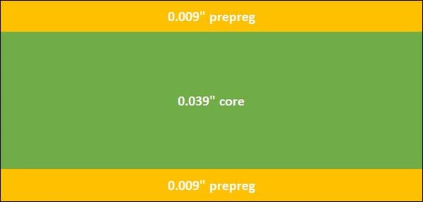
0.47" - 6-Layer PCB Stack-Up

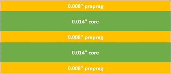
0.62" - 6-Layer PCB Stack-Up
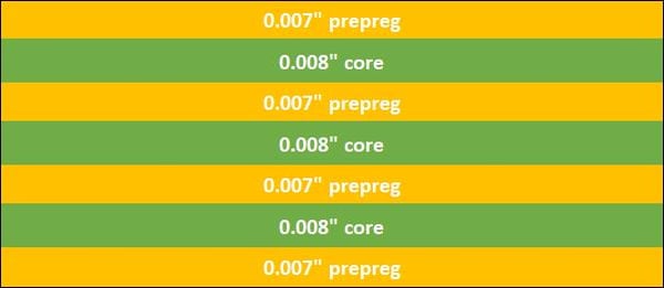
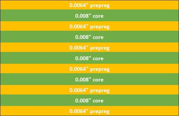
0.62" - 8-Layer PCB Stack-Up
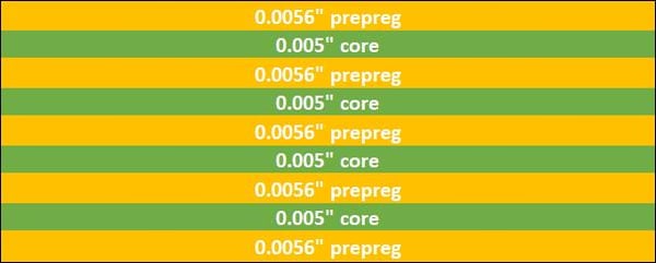
0.62" - 10-Layer PCB Stack-Up
0.93" - 12-Layer PCB Stack-Up

Summary
It is important to understand that multilayer PCC stack-up design is a very deep topic with almost limitless potential for variation. The example stack-ups herein are not intended to cover PCBs that have critical requirements related to controlled impedance, low signal loss, EMI shielding, etc. Instead, consider them to be useful and inexpensive solutions for defining the materials required for basic multilayer boards. They will help you as a designer to understand how your new PCB will be built, while ensuring consistent results, no matter where your boards are built.
Key Takeaways
- Defining a stack-up avoids variation: Without documentation, different fabricators may use different material sets, leading to inconsistent PCB performance.
- Balanced construction matters: It ensures dielectric layers mirror each other around the Z-axis center, improving stability, though thickness may not be identical.
- Foil construction is preferred: Most modern fabricators use foil with prepreg to bond copper layers, offering greater ease of manufacture compared to full-core builds.
- Specifying stack-ups simplifies quoting: Documented stack-ups allow fabricators to bid apples-to-apples, making it easier to compare costs and ensure consistency.
- Standard stack-ups cover basic needs: While not meant for advanced designs requiring impedance control or EMI shielding, they provide reliable, low-cost solutions for general multilayer PCBs.


