


Owing to the prevalence of complex processors, USB devices, and antennas printed directly onto the board surface, more and more PCB designs now require impedance control and testing than ever before. In response to the increased demand, circuit board manufacturers have invested in sophisticated modeling software and testing units, so they are equipped to meet the requirements.
It is important, however, for PCB designers to understand the best way to communicate their expectations when creating documentation. A missing piece of information, even if it seems small, can make it difficult or impossible for the fabricator’s engineering group to know exactly what the customer needs.
Controlled impedance affects the combination of material types and thicknesses the fabricator will need to use in order to hit the target impedance, as well as any micro-adjustments that may be required to the Gerber files in pre-production. If the impedance callouts are unclear, then it becomes impossible for the fabricator to plan the order, because the bill of material (BOM) is not known. The order ends up being held in pre-production until the missing information arrives.
Fortunately, it is not difficult to specify your impedance requirements clearly. The first step is to understand which pieces of information you need to supply so that your order will proceed smoothly, without delays.

Parameters to Specify
Before stating the impedance requirements, be sure to include accurate callouts for material type, copper weight, and number of layers. You may supply these callouts within a formal fabrication drawing that includes graphics, or as a simple README text file. Be sure that the information you are adding is specific to the design at hand. Importing a generic stack-up view that does not match the current design’s requirements will confuse rather than illuminate.
Similarly, if you require that a material be used, be sure to make that clear. If you don’t necessarily need a particular product but do need the fabricator to use a material with specific properties such as low Dk and / or Df, include those properties as part of your specification as well. All of these items are potentially useful for the manufacturer’s front-end engineers, no matter what type or class of PCB you are ordering, but they take on greater significance when you need to meet an impedance target.
If a PCB has been designed correctly, and the basic material callouts are comprehensive, there are just a few additional parameters to consider when it is necessary to control impedance. The absolute basics are target impedance, trace width, trace height, and Z-axis distance from the trace across the dielectric layer to the reference plane, if known. For differential or coplanar calculations, it is also necessary to know the copper-to-copper spacing for the controlled traces. Even at its worst, it’s not a long list, and it is made up of things that have already been considered during the design stage. Surprisingly, though, these requirements don’t always end up on the PCB documentation when the board goes for production. In most cases this is simply an oversight, and one that can be remedied without too much extra work.
Incomplete Information Causes Delays
As an example of the problems caused by incomplete information, let’s look in on a front-end pre-production engineer, who is preparing your 6-layer PCB Gerber files for production using CAM software late one Friday afternoon in June. In this example, we will say that the job originated as an online order, which means the engineer is the first person in the fabricator’s organization to review the data files. The drawing notes appear to be reasonably complete – copper weights, mask color, surface finish, etc. are all there. So far, so good, it would seem. But the devil is in the details.
The next note specifies impedance control: single-ended 50 Ohms, and differential 100 Ohms. A glance at the drawing shows that the 6-layer PCB consists of four signal layers, and two planes, arranged as TOP, GND, SIG3, SIG4, PWR, and BOT. The engineer wonders: Is impedance control required for all four signal layers? Or if not, then for which individual layers? And what trace width needs to be controlled?
Remember that the answers to these questions will dictate material selection, CAM data adjustments, artwork scaling, and design of the impedance coupons. Now we see the CAM engineer composing an on-hold notification before going on to the next order in the work queue, instead of tooling your order for manufacturing. Hopefully the PCB designer hasn’t left for a two-week vacation in a place with no cell phone service, or the order may remain on hold for a while. With only slight variations, this scenario is all too common.
Nailing Down Your Impedance Expectations
The impedance requirements could have been much clearer had the note included just a little more information. It could have said something as basic as the following:
Impedance control required: For TOP layer, 0.006” trace / 0.006” space = 100 Ohms differential, +/-10%, ref to L2/GND. For TOP layer, 0.0095” trace, single-ended microstrip, ref to L2 GND.
Or:
Impedance control required: L1, L3, L4, L6, 0.005” trace / 0.005” space = 100 Ohms differential +/-10%. L1 and L3 ref to L2. L6 and L4 ref to L5. TOP layer 0.008” trace, single-ended microstrip 50 Ohms +/-10% ref to L2/GND.
These notes are not exactly long and complicated, yet everything is now clear – the target impedance, the trace / space geometries, which layers use those geometries, and which planes serve as reference layers for the various signals. The order which could have ended up on hold is now on its way through manufacturing.
You can also supply a full table showing all the layer thicknesses, copper weights, trace widths, and impedance targets, as shown in the illustration. Now that we have an example of a good set of impedance notes, we can wrap up with a short list of things we recommend against doing.
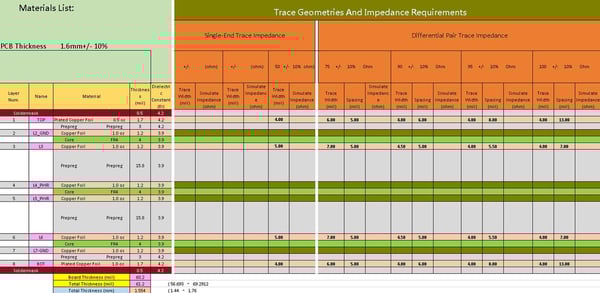
The above table is very comprehensive and can be adjusted to cover several trace geometries and different impedance requirements clearly.
Avoiding Common Mistakes
Here is a list of impedance-related notes we have seen that can also cause confusion or on-hold situations:
- Only one trace width can meet a particular impedance on any one layer. It is not sensible to expect, say, a 0.007” trace and a 0.005” trace to both solve for 50 Ohms on the same layer. Although this seems painfully obvious, we have seen instances where the requirements were called out in this manner. It does not work. Only one trace width or pair geometry can meet a particular target impedance per layer.
- If you have a dense 16-layer board, and your note reads: “All signal layers: 0.004” trace, 0.006” space to be 100 Ohms differential” please make sure that the specified geometry is present on ALL the signal layers. If it’s not, then clarify by specifying only the layers where the geometries exist. Searching through 8 or 10 dense signal layers with hundreds of seemingly parallel 0.004” traces in search of a few true differential pairs is tedious enough, but searching all those layers to discover that there are 0.004” / 0.006” pairs on just ONE of the internal layers wastes significant time. It is also necessary, once the weeding-through is completed, to document that impedance testing may be waived for layers not using those pairs. Otherwise an incoming inspector will reject the impedance report when the boards arrive, on the grounds that it is incomplete as defined by the drawing note. Therefore, it is important that you identify only those layers that actually use the specified trace geometries.
- If you supply a reference stack-up, it is good practice to also state clearly whether or not you permit adjustments to meet the impedance targets. Some drawings arrive with generic stack-ups included, which will not serve to meet the custom requirements of a controlled impedance PCB. If the notes do not make it clear that adjustments are permitted, then the fabricator has no choice but to stop the order and seek your permission to deviate from the supplied stack-up.
- Impedance tolerances tighter than the standard +/-10% will often be the source of questions. The reason is that while tighter tolerances are possible, they come at a cost, because a greater percentage of otherwise-perfect product may be scrapped for relatively small impedance-related nonconformances. The majority of these more stringent tolerance callouts are the result of authors who are simply not aware that +/-10% is standard, so they put other values on their drawings. Fabricators ask because they need to know whether or not a tighter tolerance is actually required, so they can price the work accordingly.
- The final mistake is actually two mistakes, which sometimes occur separately, and sometimes together. One, already touched upon above, is importing a generic stack-up into your CAD drawing that does not match your current design. The other is adding requirements in your NOTES section that do not match the information in your stack-up view. This sort of contradictory information is probably the single most common reason that multilayer PCB orders are held up, whether or not impedance control is required. It is well worth taking a few minutes to review your notes versus your stack-up and be sure to resolve any mismatches you find.
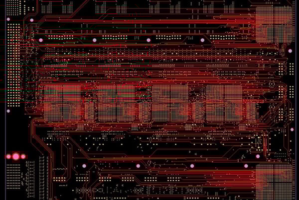
Above image illustrates all traces on this large PCB are the same size. Identifying the pairs among so many parallel lines is difficult and time-consuming.
Clear Requirements Keep Things Moving
When your high-tech PCB requires impedance control in order to function correctly, it is important to state the requirements as clearly as possible in the accompanying documentation. A note that includes all the relevant parameters will minimize questions and prevent delays.
When the requirements are clear, the PCB fabricator can easily verify that the Gerber files and the stack-up will combine to produce the correct result. That means there will be no delays in material ordering, no time wasted exchanging emails or phone calls, and no reason for your PCBs to be built out of spec on account of a missing piece of information.
Spending a few minutes ahead of time double-checking to be sure that everything matches will pay dividends in the long run. Instead of unexpectedly needing to drop what you are doing later to clarify a requirement that’s missing from the board specification, you will be able to go about the business of completing your next PCB design while fabrication proceeds uninterrupted on your last one.

Summary
As more PCBs are designed for high-speed applications involving USB, RF, and antenna components, controlled impedance is becoming a standard requirement. However, incomplete or unclear impedance specifications in design documentation can lead to production delays, incorrect material choices, and failed performance targets.
To avoid these issues, PCB designers must provide complete and accurate impedance details, including trace width, spacing, layer references, and tolerance expectations. Simple, precise callouts ensure fabricators can move forward confidently, minimizing back-and-forth and keeping the order on schedule. When properly specified, impedance control adds performance, not production headaches.
Watch Our Controlled Impedance Video Series
Part 1: Understanding the Stack-Up in Impedance Calculations
Part 2: Gerber Data
Part 3: Impedance Validation
Key Takeaways
- Clarity Prevents Delays: Always specify which layers require impedance control, the trace dimensions involved, and their reference planes. Vague or generic notes are a major cause of stalled production.
- Supply All Critical Parameters: Include key variables like trace width, spacing (for differential pairs), copper weight, dielectric thickness, and target impedance values. These details are essential for accurate modeling and coupon design.
- Avoid Stack-Up Mismatches: Imported or generic stack-up diagrams must reflect the actual design. If deviations are allowed to meet impedance targets, explicitly state that on the drawing.
- Stick to Standard Tolerances: Unless truly necessary, use the industry standard ±10% tolerance. Tighter specs increase costs and scrap rates, often without meaningful performance benefit.
- Consistency Is Crucial: Ensure your notes match your stack-up. Conflicting details between documentation sections is a top reason for production holds and can lead to costly errors or redesigns.


