


The design of a multi-layer PCB (printed circuit boards) can be very complicated. The fact that a design even needs to use more than two layers implies that the required number of circuits will not fit onto just a top and a bottom surface. Even in cases where the circuitry does fit onto two external layers with no problem, the PCB designer may decide to add power and ground planes internally in order to correct a performance shortcoming.
There are many different factors that can cause a circuit to perform less than optimally, from thermal issues to complex EMI (electromagnetic interference) or ESD (electrostatic discharge) problems that need to be chased down and eliminated. But while as a designer your top priority is to correct electrical problems, it is just as important not to lose sight of the board’s physical configuration. A board that is electrically flawless may still bow or twist, making assembly difficult or even impossible. Fortunately, attention paid to the PCBs physical configuration during the design cycle will minimize assembly headaches later. Layer-to-layer balance is one of the key aspects of a mechanically sound circuit board.

A Balanced PCB Stack-up
A balanced stack-up is one in which both the layer surfaces and the cross-sectional structure of the printed circuit board are reasonably symmetrical. The goal is to eliminate areas which could deform when subjected to the stresses of production processing, particularly at the lamination stage. When a circuit board deforms, it can become very difficult to get it to lie flat enough for assembly. This is especially true for boards which will be assembled on an automated surface mount pick and place line. In extreme cases, deformation could even hamper installation of the populated PCBA (printed circuit board assembly) into the final product.
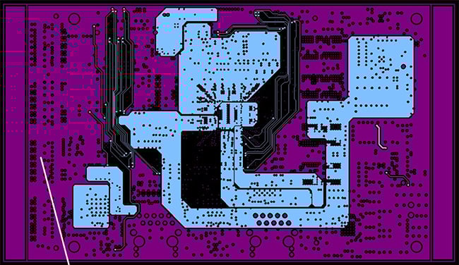
PCB with copper poured to reduce bow and twist.
There are IPC inspection criteria that should prevent the most seriously bowed or twisted boards from ever arriving at your facility. Still, if the PCB fabricator’s processes are not wildly out of control, the root cause of most bow and twist turns out to be design related. For that reason, it is advisable that you perform a thorough review of the PCB layout, and make any necessary adjustments, before placing your first prototype order. Doing so may prevent a poor yield.
Circuit Board Cross-Section
One common design-related reason that a printed circuit board will not finish acceptably flat is that its cross-sectional structure is not symmetrical about its center. If, for example, an 8-layer design uses 4 signal layers or partial planes with relatively light copper coverage above the center, and 4 relatively solid planes below, then the stresses exerted by one side of the stack versus the other will probably cause the entire stack to deform when the materials are laminated using heat and pressure after etching.
It is therefore good practice to design the stack-up so that the type of copper layer (plane or signal) is mirrored in relation to the center. In the diagram below, the top and bottom layer types match, as do those for L2-L7, L3-L6, and L4-L5. Presumably the copper coverage is comparable on all the signal layers and the plane layers primarily consist of solid-poured copper. If so then the board has a good chance to finish with a flat, even surface that will be ideal for automated assembly.
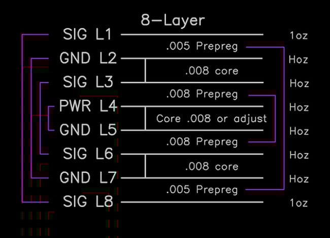
Symmetrical PCB stack-up with balanced plane and signal layers.
PCB Dielectric Layer Thickness
It is also good practice to balance the dielectric thicknesses throughout the stack. The thickness of each dielectric layer should ideally be mirrored in a manner similar to the way that the layer types are mirrored.
When the thicknesses are not the same, it can be difficult to arrive at a material set that will lend itself to easy manufacture. Sometimes an asymmetrical stack-up is unavoidable, on account of a feature such as an antenna trace which may need an unusually large distance between it and its reference plane but be sure to explore and exhaust all other options before moving forward. Most fabricators will request a relaxation or outright waiver of the bow and twist tolerance when uneven dielectric separations are required and may even walk away from the work if they cannot get such a waiver. They do not want to find themselves rebuilding several costly batches at low yield before finally getting enough good units to satisfy the original order quantity.
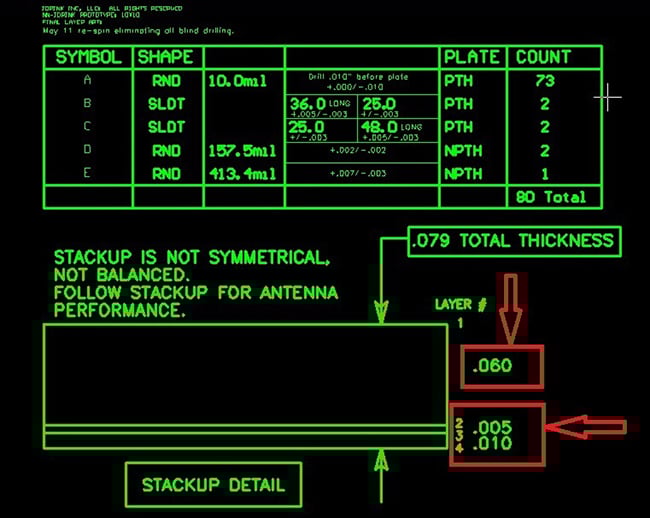
Example of an asymmetrical PCB stack-up.
PCB Thickness Issues
While bow and twist is the most common quality problem that occurs when your stack-up is not balanced, there is another condition which can occasionally cause disputes at final inspection – variation in overall PCB thickness at different locations on the board. This condition is brought on by a seemingly minor design oversight, and is relatively unusual, but it can happen if your layout includes consistently uneven copper coverage in the same location on several layers. It is mostly seen on boards which use at least 2-ounce copper and relatively high layer counts. What happens is that one section of the board has a significant area of poured copper, while the other section is relatively devoid of copper. When the layers are laminated together, the side with the copper presses down to one thickness, while the side with light or no copper ends presses thinner.
Most boards that use half-ounce or 1-ounce copper won’t suffer much, but the thickness loss with heavier copper can be significant. If you have, for example, 8 layers of 3-ounce copper, the zone with the lighter copper coverage can very easily fall below the overall thickness tolerance. To prevent this from happening, be sure to pour your copper as evenly as you can across the layer surfaces. If this is not practical on account of either electrical or weight concerns, then at least add some plated through holes to the light copper zone and be sure to include pads for the holes on every layer. These hole / pad structures will provide mechanical support in the Y axis, thereby reducing the loss of thickness.
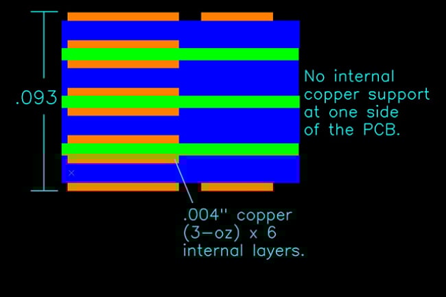
8-layer 3 oz PCB with uneven copper coverage.
Compromise for Success
It is important to pay attention to both electrical performance and physical structure when designing and laying out a multilayer PCB, even if you need to compromise slightly on both aspects in order to arrive at an overall design that is both functional and manufacturable. As you weigh your options, keep in mind that a design with perfect electrical characteristics will not be of much use if it is difficult or impossible to populate with components on account of deformation in the form of bow and twist. Balance your stack-up and pay attention to copper distribution on the various layers. These steps increase the likelihood that you will end up with a board that is easy to assemble and install.

Summary
Balancing your PCB stack-up is essential not only for electrical performance but also for ensuring a physically stable and manufacturable board. As layer counts and copper weights increase, asymmetrical layouts can lead to bow, twist, and inconsistent thickness issues that compromise automated assembly and final product integration.
By mirroring signal and plane layers, matching dielectric thicknesses, and distributing copper as evenly as possible, designers can avoid costly fabrication problems and improve overall yield. A well-balanced stack-up is key to producing a reliable, flat PCB that performs as intended and assembles without complications.
Key Takeaways
- Layer Symmetry Prevents Warping: A balanced PCB stack-up, with mirrored layer types and copper weights across the center axis, helps prevent bow and twist during lamination and ensures better flatness for assembly.
- Copper Distribution Impacts Flatness and Thickness: Uneven copper coverage across layers or specific board regions can cause deformation or local thickness variation, especially in high-copper, multi-layer PCBs.
- Dielectric Thickness Should Also Be Balanced: Mirroring dielectric thickness across the stack-up is crucial. Uneven dielectric layers can complicate manufacturing and may result in bow and twist that exceed IPC tolerances.
- Manufacturability Can Trump Electrical Perfection: While electrical performance is vital, compromising slightly to improve mechanical balance can result in a design that is both functional and manufacturable at scale.
- Use Copper Pours and PTH Strategically: When copper weights must vary, using copper pours and adding plated through holes with pads in low-copper areas can improve mechanical stability and maintain board thickness tolerances.


