


Ordinarily you may not want your PCB (printed circuit board) manufacturer to adjust your data files, but there are occasions when that may be the easiest way to achieve a particular result. For instance, you may need to have some, but not all, vias of a particular size plugged so that the assembly solder will not wick through to the other side of the board. Or perhaps a few trace pairs need to run at a specified impedance, while the impedance for all the other traces of the same width is non-critical.
For one reason or another – usually a lack of available space – you may not be able to make these “special” features a different size from the rest. Your circuit board fabricator may then struggle to differentiate between what is special versus what is standard, especially on large, dense designs, because everything is the same size.
An easy fix is to make a 0.0001” size adjustment to your special features. Such a small difference will be insignificant in terms of performance but will help the fabricator understand where the critical features are located and to quickly manipulate the data to get the result you need.

Differential Impedance Traces
Impedance controlled traces are generally straightforward, as long as you define your target impedance, trace size, and layer where they can be found. The fabricator’s CAM (computer-aided manufacturing) engineer will use this information first to identify the traces by feature size, then to apply micro-adjustments as needed so the impedance will run as close as possible to the nominal value. Even with clear callouts, however, differential pairs can still be tricky to find if the same feature size is also used for other non-critical traces on the same layer. The first step for the CAM engineer is to find the locations where differential pairs are present, so that they can be adjusted if necessary.
Assuming that you have stated your impedance requirements clearly and used a unique aperture size to define the differential pairs, the CAM engineer will attempt to identify and highlight the D-code for the appropriate feature size, making it highly visible. Then, having found the highlighted code, they will zoom to measure between the traces in order to verify that the spacing of the critical pairs matches the drawing note. If adjustment is required, they will be able to select all the traces on the entire layer, using a filter to select by size. They can then adjust the trace width without affecting any other features. For many designs, this is exactly how the verification and adjustment process play out.
On the other hand, consider a scenario where most of the traces on a particular layer are all drawn the same size as the critical pairs. Maybe the layer uses a single aperture, such as a 0.005”, for nearly all the circuitry, and the layer is fairly large and dense. Simply finding the 0.005” D-code in the aperture table and highlighting it on-screen will not help very much on a layer like this. The entire layer will light up, presenting the engineer with a seemingly undifferentiated maze of 0.005” traces, many of which appear to run at least approximately parallel.
Since there is no “select all differential pairs” editing command, it will be fairly tedious to pan and zoom all around the layer in search of what might turn out to be just one or two true differential pairs. Nevertheless, it is essential to know where the pairs are located, so that it will be possible to make necessary micro-adjustments later, without affecting any other features. It might seem easy enough at first to take a shortcut, by simply adjusting all of the 0.005” traces on the entire layer and be done with it.
Why not just do that?
The answer is that when all the 0.005” traces are made larger, the amount of increase to their size brings with it a corresponding decrease to the spacing between those traces and all of the adjacent copper features on the layer. On a dense circuit board, where the design spacing may already be at the minimum acceptable value, this could introduce a fair number of design rule errors for minimum spacing violations. The design rules are in place to guarantee that the finished PCB will be manufacturable, and that the result will be repeatable, so pushing the spacing below the established process limits across the entire layer will adversely affect the production yield. It is much more sensible to adjust only those features which need adjustment, and to leave the rest alone. This is the main reason why the CAM engineer will seek to identify and adjust only the critical pairs, without affecting the other 0.005” traces.
How can the PCB designer make the critical traces easier for the cam engineer to find?
One simple solution that does not require searching by net names or component reference designators is to change the feature size of the critical circuits by 0.0001”. In the example above, the traces used in the differential pairs could be decreased from 0.0050” to 0.0049”. Now, even on a large, dense layer swarming with 0.005” traces, the relatively few 0.0049” traces will be easy to find by the highlighting method. Even if the minimum trace DRC (Design Rule Check) value for the layer is 0.0050”, the presence of a few 0.0049” traces will produce only a handful of violations.
Besides, impedance-controlled traces almost always require micro-adjustments to their size so that they will solve as close to the nominal impedance value as possible. In the end, the 0.0049” traces could very well end up being plotted for production at, for instance, 0.0053”. At that point they would no longer represent a violation. The point is that making the traces easy to identify is more useful than splitting hairs over a tenth of one thousandth of an inch of width.
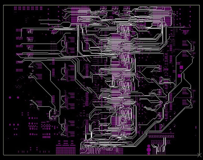
Example of PCB layer with an unspecified quantity of differential pairs. All traces are 0.006”.
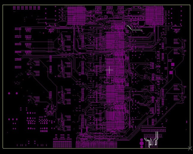
Example of PCB layer that has segregated differential pairs as 0.0059” to make them easy to find.
Vias
Another similar 0.0001” adjustment can help to identify special requirements for a certain subset of your drilled vias. In one common scenario, you may want the PCB fabricator to use an extra application of solder mask to plug some, but not all, vias of a particular diameter. If you are unsure about how to go about modifying your own Gerber layers to represent this special processing and prefer to have your fabricator’s engineers apply their expertise to get the correct result, then you can supply special instructions instead of Gerber files.
For example, your circuit board design may use a single via diameter of 0.008”. All the vias have solder mask openings around them. After a bad experience with solder wicking away through certain vias on a previous revision, you decide to add a note so the fabricator will plug those vias with mask. The problem is that you do not know how to make a Gerber layer to get this result, so you add a note stating that the fabricator should “use solder mask to plug all thermal vias.”
While there is nothing inherently incorrect about this note, it does leave some room for misinterpretation. First is that nothing specifically defines what you mean by the term “thermal vias.” And since all the vias are the same diameter, you have left it to the fabricator to determine which specific holes you’re talking about. What usually happens next is that the fabricator’s CAM engineer will overlay the paste layer with the drill and scan around the design to visually identify the large pads at the centers of your QFPs (Quad Flat Packages) and similar devices. Once they have done so they will often send you a screen shot of the holes they’ve found for confirmation that they’ve found the right ones.
This series of steps will work, but it is clunky and takes time. Assuming that you know which vias have a “thermal” function, you also know where they are located. A better strategy – one which would eliminate both guesswork and approval – is to segregate the thermal vias onto their own drill tool. If you need or want all the vias to be the same size, to meet either current carrying requirements or real estate limitations, then you can do the same thing you did with the differential traces, by applying a 0.0001” reduction in the drill diameter. Now you can change the note to something like: “Plug all 0.0079” diameter vias from bottom side.” This will make it simple for the CAM engineer to use selection filtering to copy only that hole diameter to a blank layer which can then be adjusted to meet the plugging requirement.
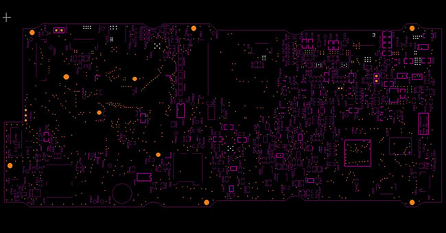
Example of certain vias plugged and separated them to make their locations clear.

Summary
It’s not necessary for you as the PCB designer to understand exactly what your fabricator does at every single production stage, or to provide perfect, production-ready photo tool files for every special process. Still, a few clear notes and a handful of minor data edits will increase your chances at success. If you find that you need to stray from your comfort zone, ask your PCB fabricator for advice about how best to express your needs so that your order will come out the way you want it, without mistakes or delays.
Key Takeaways
- Use Micro Adjustments to Highlight Critical Features: Applying a slight size change (like 0.0001”) to critical vias or impedance-controlled traces helps PCB fabricators easily identify special features without impacting performance or design integrity.
- Avoid Mass Adjustments That Risk Design Rule Violations: Instead of adjusting all traces of the same size, isolating only the necessary differential pairs prevents unintended spacing issues that could lower manufacturing yields or cause non-compliance with design rules.
- Simplify Communication with Fabricators Using Clear Data Cues: Small, intentional variations in feature sizes, paired with clear notes, remove ambiguity, making it easier for CAM engineers to process special requirements like via plugging or impedance control without back-and-forth clarification.
- Enhance Efficiency by Segregating Special Vias: For vias requiring unique processing (e.g., soldermask plugging), slightly reducing the drill size allows fabricators to filter and apply treatments efficiently, eliminating guesswork and reducing lead times.
- Collaborate with Your PCB Manufacturer for Custom Solutions: You don’t need to master every fabrication detail; simple design strategies and open communication with your PCB supplier will ensure special requirements are met accurately, minimizing errors and delays in production.


