


There was a time when the PCB manufacturing industry included a fair number of bucket shops, so called because much of their processing was done in small portable tubs filled with etchants, solvents, and other mysterious solutions. They cranked out very basic, low-cost, low-complexity PCBs, using equipment and methods that were questionable at best. Their business and environmental practices were often similarly questionable.
The good news for circuit board customers is that bucket shops are a thing of the past. Those fabricators who remain viable can execute all basic production steps repeatedly, with a low likelihood of scrap, on printed circuit boards that would have been considered insanely complex just a few years ago. Still, there are higher-end processes that not every supplier is equipped to do.
It is important to be sure that the circuit board you are about to order is going to a PCB manufacturer that can handle several difficult design features simultaneously. Otherwise your order could be scrapped, or it could show up on your dock with undetected manufacturing errors that will complicate assembly, installation, or function. The following post explains what some of the more difficult processes are, so that you can be sure to identify an appropriate fabricator for your order.

Controlled Impedance
There was a time when many small to medium shops were not able to support impedance testing, but those days have passed. Controlled impedance PCB designs are now so common that the ability to check impedance results has become a basic requirement for remaining in business. It is now possible to have your order tested no matter where it is built. If you supply the necessary information at the beginning of your project, your boards should arrive with a report of the results. Expect to pay a small up charge per PCB. The up charge covers the cost of setting up and performing the test, which is not done on the same machine as the one used for checking basic continuity. It also covers the potential small increase in fallout for boards which fail impedance testing, despite being free of other manufacturing errors.
Wraparound Edge Plating
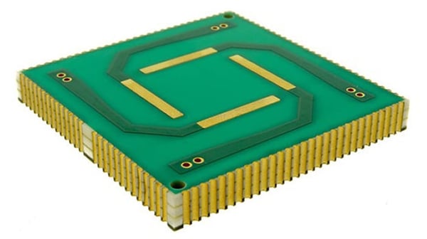
Occasionally, it is desirable to form a connection by wrapping the plating around the PCB edge, rather than by means of a standard via hole, so that the edge can serve as a conductor. The fabricator accomplishes the wrap plate by performing an extra primary routing operation immediately after drilling. The purpose of this routing step is to expose the PCB sidewall so that it can be coated with electroless base copper (or an equivalent) in the same manner and at the same time as it is applied to the drilled holes.
After the photographic circuit image has been applied and developed, the electroless layer provides a conductive surface onto which the thicker, more durable electrolytic copper can adhere. If the artwork includes a pad or other shape that defines the routed area as a plated feature, the electrolytic copper plating will coat the routed channel to form the desired connection. While this process adds steps, plus a small amount of complication in the planning of array setups and machining processes, it is not overly difficult to arrive at a good result.
Printed circuit board with wraparound edge plating.
Castellated Edge Plating
Related to wraparound plating, castellated edge plating involves plating a series of holes that have been drilled so that their center points fall along the PCB outline. The holes are later routed through so as to leave behind plated half-holes with space between them. Castellations are most often used to facilitate the mounting of a pre-assembled module to either a small breakout board or to an area of a larger board. The half-holes on the castellated board are usually spaced to align with surface mount pads on the larger board. When the two boards are joined, the plating in the barrel of each half-hole provides an extra mating surface for soldering. The assembly solder wicks up the barrel of the half-hole, resulting in a joint that is more secure than a basic butt joint.

While castellations are quite useful, not every fabricator has a repeatable process for forming them on the bare printed circuit board. Considering the small holes that are usually used, and the tight tolerances that apply to each of the constituent operations, it is very easy to arrive at a less than optimal result. The most common problem is that the half-holes can end up misaligned to the PCB edge because of small shifts in registration that occur during various setup steps in the production sequence. The result is a smaller than desired surface area for soldering to the hole’s sidewall along one or more edges.
Another problem is that copper can sometimes pull free from the substrate at the unsupported side of the hole during final routing. The routing tool then drags what had previously been the round hole’s sidewall plating until it curls around into the center of the half hole, forming an obstruction that is nearly impossible to remove without damaging the layer-to-layer interconnection. If you plan to use castellations, be sure to ask the PCB manufacturer to demonstrate that they have a good process in place to prevent such mishaps.
Printed circuit board with castellated edge plating.
Plated Cavity
A cavity is a recessed opening which allows a component to be placed on a layer other than the top or bottom – essentially a cutout which does not pass all the way through the board. Although cavities can be used for sophisticated RF purposes, and as aids in thermal management, they are most commonly used to save physical space. Components mounted inside of recessed cavities effectively reduce the height of the PCBA. The advantage is that the assembled board will now fit within a slimmer enclosure.
Other more advanced cavities allow for components to be completely embedded. After the component is installed into the cavity, additional materials are laminated over its top, sealing it within the multilayer structure. Placement of the component inside the board frees up space on an external layer, allowing for placement of additional components or circuitry, or for making the board footprint smaller.
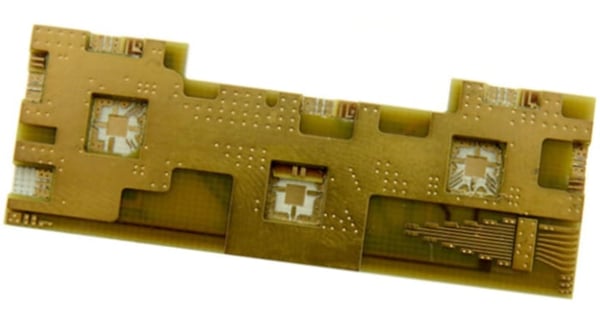
Printed circuit board with plated cavities.
Cavity formation requires experience with lamination processes and materials selection. The more consistent the layer thicknesses are, the easier it will be to control the depth of the cut. Accurate machining of the cavity is also critical. Given inevitable variations in material thickness and CNC machine setup, plus the roughness of the copper surface after mechanical milling, it is often necessary to replace mechanical milling with a more controllable laser ablation step.
Laser ablation removes the dielectric material completely, and without chatter marks, leaving the internal layer’s copper surface clean and smooth enough for reliable component mounting. If the layer to be exposed is deep within the PCB structure, then an initial CNC milling step may still be useful. The CNC pass reduces the thickness of the dielectric material in order to shorten the laser cycle time. Then the laser removes the remaining dielectric material for a clean surface. At each step, a good result depends upon the board manufacturer’s equipment, skill, and experience.
Microvias And Sequential Lamination
Microvias are very small holes that are drilled from one layer to an adjacent layer to form an interconnection that does not pass through the board from top to bottom, like a normal plated through hole. Their small size (typically 0.003” to 0.004”) makes it possible to place many holes within a very small area, thereby allowing for high density circuit routing, specifically near high pin count components such as ball grid arrays (BGAs). They are formed in most cases by laser drilling. If the microvias only connect from an external layer to the adjacent internal layer, then it is possible to form these blind vias after all lamination is complete. For more complex high-density interconnect (HDI) boards, however, additional lamination steps are required.
Sometimes microvias connect between different layer pairs at different locations (for example, some holes from L1-L2 and others from L2-L3) while other times they may be drilled in the same location at different times, in order to form “stacked” microvias. An example of the latter would be a structure designed to connect L1-L3.
The challenge is that laser microvias cannot penetrate very deeply. Because of their small diameter and their “V” cross section, the aspect ratio between hole diameter and dielectric thickness should be less than 1:1. Otherwise, the bottom of the hole will not remove all of the dielectric material required to expose the adjacent layer’s copper surface, and it will not be possible to plate the hole reliably. It is necessary, then, to stack multiple laser microvias on top of one other in the same position to connect multiple layer pairs while using the smallest possible diameter holes at the same location (or very close to one another, using an elongated capture pads). The most common feature driving such HDI structures would be a dense, high pin count BGA, where there is no space to run escape routing on the external layers alone.
To do this requires sequential lamination, where several layers are laminated together into a sub-structure and blind drilled. Then they are capped with the next set of layers, laminated, and blind drilled again. For example, a 10-layer board might have a sub-lamination comprised of L3-L8. This sub is laser drilled down one layer from both sides, then plated to connect L3-L4 and L8-L7. Then L2-L9 are added, laser drilled to connect L2-L3, and L9-L8, and plated. Finally, L1 and L10 are added, laser drilled, and plated. Now there are connections from L1-L4, and from L10-L7. If necessary, circuitry or solid poured copper can now be added in the same locations as the vias on layers 5 and 6, because there is no through via structure taking up the space.
In order to perform the steps required for successful HDI/sequentially laminated products, all machines must be well-calibrated, and all processes tightly controlled because the cost of a scrap and restart is high. As circuit boards become increasingly dense, it is important for the manufacturer to have the right equipment and experience required to produce today’s complicated multilayer structures.
Vias In Pads
Most HDI designs require that vias be drilled into the actual component pads so that it is not necessary to run extra circuitry and pads simply in order to place vias. The problem is that the drilled via hole cannot remain in the pad center on the finished PCB. If the hole is left open, then there will be little or no surface area for soldering, and what solder is applied will simply wick down through the open via hole, resulting in a poor solder joint. The solution is to fill the via, then plate over it to recover the pad area for SMT soldering. The process is sometimes known as Via-In-Pad-Planarize-Over-Plate (VIPPO) and the resulting via is known as an IPC Type VII via, also called an “active pad.”
The vias are drilled as a separate operation, before the other plated through holes, so that only the vias will be filled. The vias are plated, then filled with either a conductive or non-conductive epoxy. The panel is then sent through a planarizing device to level any areas where epoxy may be protruding from the surface, since a component such as a BGA must mount to a flat, uniform surface in order to prevent assembly problems.
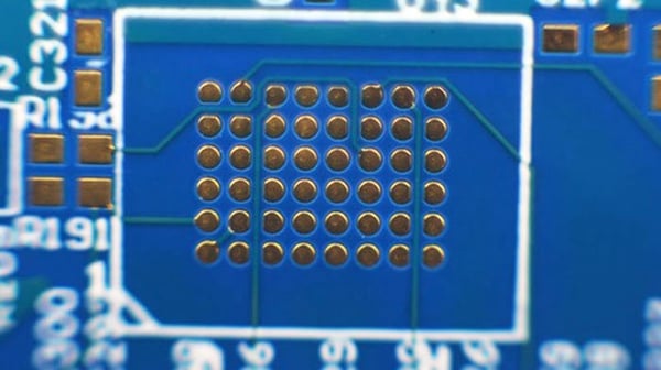
Printed circuit board with via-in-pad.
Conductive fill materials use metallic particles suspended in epoxy. These epoxies are costly, and have limited shelf life once opened, so you end up paying for the whole container even if you don’t use very much material. Most fabricators will suggest substitution of a non-conductive fill. Not only is non-conductive fill less expensive, but because there are no particulates, it is also easier to achieve a void-free fill. If loss of thermal conductivity is a concern, increasing the hole wall plating requirement from Class 2 to Class 3 will usually make up the difference. Copper is many times more thermally and electrically conductive than the filler anyway (250W/mK vs. 3-to-15W/mK) so an individual via plated with Class 3 copper and filled non-conductive epoxy should be at least as efficient as one plated to Class 2 and filled with expensive conductive material.

Summary
None of the processes described above are impossible, but they do require specialized equipment and a certain amount of attention and experience. When you put a higher technology PCB out for bids, not every fabricator will want the work. Some may lack either the equipment required to perform the more difficult steps, or the process controls required to do them repeatably. If you need to source a highly complex board that uses one or more of these advanced design features, it is well worth asking ahead of time whether or not your usual supplier is confident that they can execute the steps required to build such a board correctly. If the answer is no, then you need to identify a PC supplier with higher-end capabilities who can do the work correctly and deliver it on schedule.
Key Takeaways
- Controlled impedance testing is now standard practice but requires upfront design data and often comes with an added cost per board to ensure accurate signal integrity.
- Wraparound and castellated edge plating expand connectivity options, though they demand precise routing and plating processes to avoid defects such as misalignment or copper pull-away.
- Plated cavities reduce component height and free up board space, but they require tight process control, often combining CNC milling with laser ablation for reliable results.
- Microvias and sequential lamination enable HDI designs, especially for dense BGAs, but these processes are complex and rely on specialized laser drilling and multi-stage lamination.
- Via-in-pad technology improves assembly density, with non-conductive fills preferred over costly conductive materials for better manufacturability and performance at lower cost.


