


Flexible circuits have two material options available to encapsulate the exposed outer layer circuitry: polyimide coverlay and flexible solder mask. While both perform the same basic function of insulating the external layer circuitry, each has different characteristics and capabilities that address specific design requirements.

Material Differences: Solid Sheet Coverlay vs. Liquid Epoxy Solder mask
The primary difference between the two materials is that coverlay is a solid sheet of polyimide while a flexible solder mask is an epoxy-based liquid cured to a hardened state.
This difference impacts:
- How the materials are processed
- Ability to define fine pitch SMT and PTH features
- Electrical insulation properties
- Stiffener application and requirements
- Robustness and long-term reliability
- Flexibility
Coverlay is the long used and preferred material throughout the industry. Its natural brown color is what is commonly seen when looking at a flex circuit. As a solid sheet of polyimide, it has the same dielectric voltage withstanding as polyimide flex cores (approx. 3KV per 0.001”), is available in a variety of thicknesses to meet tight minimum bend requirements and provides an impermeable barrier. Coverlay material comes supplied with a preattached layer of either epoxy or acrylic based flexible adhesive and is then laminated, under heat and pressure, on to the flex circuit surface, creating a permanent bond.
Flexible solder mask is essentially the same epoxy-based material as used on rigid printed circuit boards, but with the addition of a flex agent. It is applied, imaged, and developed in the same manner to create the required SMT and PTH openings. Thickness is limited to ¾ to 1 mil over the base core but will be less directly over top of traces. Due to the varying thickness, it does not provide the same level of voltage withstanding and cannot be an impermeable barrier. Coverlay is more robust and flexible than solder mask.
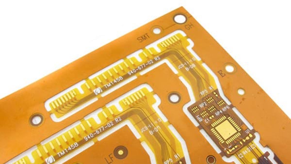
Flexible circuit board example with coverlay only.
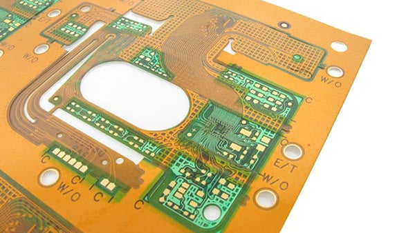
Flexible circuit board example with coverlay and soldermask.
Design Considerations
Due to the differences in the materials between coverlay and solder mask, each has different capabilities.
Coverlay, as a solid sheet of material, requires all SMT and PTH openings to be mechanically created using either laser cutting, routing or punch & die sets. This combined with the need to laminate the coverlay to the flex, limits the minimum size of openings and the minimum web of material that can be retained between adjacent openings. Excessively small coverlay webs are easily damaged or broken during processing and the limited amount of adhesive may not allow for a proper lamination. Coverlay openings may also exhibit a small amount of adhesive squeeze out into the openings. The resulting design rules for coverlay are significantly different than those for solder mask.
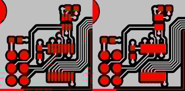
Flexible solder mask (left) and coverlay with ganged SMT openings (right).
A flexible solder mask, as a photo imaged liquid, allows for almost the same capabilities as that for rigid boards. Both materials require slightly larger feature openings to accommodate the larger material dimensional tolerances inherent to polyimide flex materials. For designs with fine pitch components, coverlay would require multiple openings to be ganged together into one large opening while flexible solder mask would typically not.
The limitation of solder mask is that it is not suitable for having stiffeners or EMI/RF shield layers thermally laminated to it. The bond strength is compromised. If a solder mask is necessary, in an area that also requires a stiffener, a PSA (double sided tape) will need to be used to attach the stiffener. For areas with shield layers, a coverlay must be used.
Thickness and Color Options
Coverlay is available in a variety of thicknesses for both the polyimide layer and the preattached adhesive layer. Standard range for the polyimide is ½ mil to 2 mil, with 1 mil being the most used. The adhesive thickness ranges from ½ mil to 2 mil, with 1 mil the most used. The adhesive thickness required is determined by the copper thickness that it is to be laminated to. The general rule is 1 mil of adhesive is needed per 1 ounce of copper. For example, 2 ounces copper requires 2 mils adhesive. This is to ensure there is enough adhesive to fully encapsulate the underlying circuitry and achieve proper lamination without voids. After lamination, a significant portion of the adhesive thickness is consumed by the filling of the spaces between circuitry, resulting in a thinner construction than the sum of all the individual material thicknesses. The polyimide layer is not affected and remains at full thickness over the traces.
Solder mask is generally ¾ to 1 mil in thickness but will be thinner directly over the circuitry. This is similar to rigid PCB processing as the liquid, after application, flows into the spaces between traces.
Coverlay is available in three colors: natural (light brown), white, and black. Natural is the most used unless there is a cosmetic requirement due to the flex being visible in the final assembly. Solder masks are available in a wider range of colors: green, black, white, yellow, etc.
Selective Application
Increasing design complexity, tighter bend requirements, and high-density components can result in designs where neither material meets the all the project design requirements. To resolve this, a common practice is to use both materials selectively applied where and as needed. This allows for the best properties of each material to be utilized. Coverlay is applied to areas subjected to bending, with large pitch components and or shield layers. Flexible solder masks are used in high density component areas.
The coverlay is applied first and the solder mask second with a slight overlap onto the coverlay to prevent any gaps in the combined layer. This method will require the input of your flex supplier to ensure a functional and reliable design that meets your requirements. The transition from coverlay to solder mask, combined with the overlap of the materials, may create a mechanical stress concentrator that could negatively affect the bend requirements and needs to be located away from tight bend areas in the design.

Summary
Polyimide coverlay and flexible solder mask provides effective material solutions to address a wide variety of design requirements. Which material or combination of materials applied will depend upon the bend requirements and component density of a specific design. Please feel free to contact Epec if you have any questions regarding selecting and applying the correct materials to your flex circuit design.
Key Takeaways
- Coverlay and flexible solder mask serve similar functions but differ in material properties: Coverlay is a solid polyimide sheet with strong insulation and durability, while flexible solder mask is a liquid epoxy-based coating that allows for fine-pitch features.
- Coverlay offers superior insulation and flexibility, making it ideal for high-reliability applications: It provides an impermeable barrier, excellent dielectric properties, and better mechanical protection than flexible solder mask.
- Flexible solder mask allows for finer feature resolution and SMT compatibility: Unlike coverlay, it can be applied in precise patterns, making it ideal for high-density PCB designs, but it lacks the bonding strength required for stiffeners and EMI shields.
- Selective application of both materials can optimize performance in complex designs: Using coverlay in bending areas and solder mask in dense component regions ensures the best mechanical and electrical properties.
- Material thickness and adhesion properties dictate design limitations: Coverlay requires precise adhesive thickness for copper encapsulation, while solder mask is thinner and available in more color options but does not provide the same level of protection or flexibility.


