Essential to any flex or rigid-flex printed circuit board (PCB) contruction is validation that your flex PCB design will meet your mechanical bend requirements. Minimum flex bend radius requirements were put in place so your design won't exceed the physical capabilities of copper circuitry, which would result in failed parts, long term reliability concerns, and several giant headaches.
So what are the types of bending forces, and how should you be preparing your flex PCB designs to handle them? The image below shows how bending a flexible circuit board creates compressive forces at the inside of the bend and tensile forces on the outside.

If the tensile stress exceeds the copper’s ductility limits, the traces will wear down, become embrittled, and lead to the formation of cracks.
Bend requirements fall into three main categories as defined by IPC 2223C Design Standard for Flex Printed Boards, all of which have their own requirements and limitations.
- Flex to Install
- Dynamic Flex
- One Time Crease
For each category, the minimum flex & rigid-flex bend capabilities are determined based on the deformation that the copper is subjected to, calculated as a multiple of the finished flex thickness. If the flex circuit is 3-layers or greater, bonded designs are required for greater minimum bend radiuses.
Flex To Install
The flex circuit is bent to a required shape and installed in the final assembly. In this scenario the flex circuit is not subjected to any further significant bend requirements.
Minimum bend radius:
- 1-2 layers = 6X
- 3 plus layers = 12X or greater
Dynamic Flex
The flex circuit is subjected to constant infinite repetitive bending as part of the operation of the final assembly.
Limited to 1 - 2 layer designs:
- 1 layer preferred
- Allows copper to reside on neutral axis of bend radius
Minimum Bend radius:
- Approximately 100X
One Time Crease
The flex circuit is bent/creased to the point of a zero bend radius, then installed in the final assembly. Creased fold is not to be opened.
Limited to 1–2 layer designs only:
- 1-layer preferred
- Allows copper to reside on neutral axis of bend radius
- Thin flex materials and copper weights required
- PSA is typically added adjacent to crease area adhere the flex to itself and prevent any further manipulation of the creased circuit.
It's noteworthy that designs can fall between the definitions of Flex to install and Dynamic Flex.
Semi Dynamic
Flex circuits are subjected to a number of bend cycles throughout their lifespan, which necessitates servicing or setting a predefined number of operational cycles. Because of these limitations, the bend radius and number of cycles should be carefully monitored. Reduced flex thickness is also preferrable to allow for sufficient safety margin and long term reliability.
Electrical Design Requirements
Certain electrical design requirements result in a thicker flex design, which in turn limits the minimum bend capabilities of the flex circuit.
Controlled Impedance:
- Thicker flex core required to allow for correct dielectric spacing between signal layers and reference planes to meet specific impedance requirements.
Current Carrying:
- May require thicker copper to meet current carrying requirements.
- Wider trace widths preferred, if available room allows, as opposed to thicker copper.
- Thicker copper requires thicker coverlay adhesive layers, to ensure full circuitry encapsulation, and further increases flex thickness.
EMI / RF Shielding:
- Requires additional external layers to provide required level of shielding.
- Layers may be either copper, silver ink or shield films.
Flex Circuit Material Selection
Standard design practice is to minimize the thickness of the flex circuit as much as practical while meeting the electrical requirements of the design and not incurring unnecessary added material costs.
As a result the most common materials are as follows (in order of preference):
- Copper Weight: ½oz , 1oz
- Flex Core Thickness: 1 mil, 2 mil, 3 mil
- Coverlay Thickness: 1 mil, ½ mil
Flex cores are also available in two different construction types: Adhesive and Adhesiveless, which based on the method used to attach the copper to the polyimide core.
- Adhesive uses a layer of flexible adhesive to bond the copper to the polyimide core
- Adhesiveless bonds the copper directly to the polyimide core
Fully Bonded vs air gap Constructions
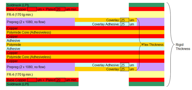
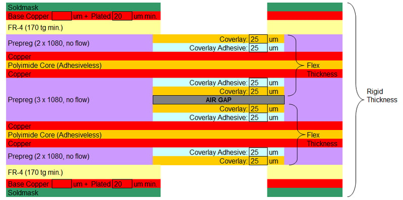
Higher layer count designs may need to utilize an Un-bonded Air Gap construction, a technique which configures layers as separate pairs, as opposed to a single fully bonded unit. The thinner individual pairs provide a higher degree of flexibility.

Illustration of Rigid-Flex Circuit Board with Bonded Layers

Illustration of Rigid-Flex Circuit Board with Air Gap Construction

Summary
The ability of flex materials and construction to meet flex PCB bend requirements is a critical element of every effective design. No matter the bend requirement category your design fits into, pushing flex materials beyond their recommended capabilities will result in problems that take time and money to fix.
For most applications, the industry has developed a wide range of design options, materials, and construction methods that can each be applied to designs cost effectively and reliably to meet bend requirements of flexible circuit boards. Learn more from our design guide below and start building the best flex and rigid-flex PCBs with Epec today!
Key Takeaways
- Importance of Bend Verification: Ensuring that a flex or rigid-flex PCB meets minimum bend requirements is crucial to preventing copper work hardening, cracks, and long-term reliability issues.
- Three Bend Categories: Flex bend requirements fall into three categories:
- Flex to Install: Limited to a single bend during installation, with minimum bend radii of 6X for 1–2 layers and 12X for 3+ layers.
- Dynamic Flex: Designed for repetitive bending, with minimum bend radii around 100X and limited to 1–2 layers.
- One Time Crease: Bent to zero radius for installation and not reopened, requiring thin materials and PSA to prevent movement.
- Semi-Dynamic Flex: For designs requiring limited bending cycles during servicing or operation, reduced flex thickness ensures reliability over time.
- Electrical Design Impacts: Certain electrical requirements can increase flex thickness and reduce bend capabilities:
- Controlled Impedance: Requires thicker flex cores for proper dielectric spacing.
- Current Carrying: Prefers wider trace widths to thicker copper for heat management.
- EMI/RF Shielding: Adds external layers, increasing overall thickness.
- Material Selection Priorities: To optimize flexibility and reduce costs, standard materials include:
- Copper weights: ½ oz and 1 oz.
- Flex core thicknesses: 1–3 mils.
- Coverlay thicknesses: ½–1 mil.
- Adhesive vs. Adhesiveless Flex Cores:
- Adhesive cores are cost-effective but less flexible.
- Adhesiveless cores provide better flexibility and durability but are more expensive.
- Bonded vs. Air Gap Construction:
- Bonded Layers: Fully laminated designs for simpler applications.
- Air Gap Construction: Thinner, independent layer pairs for higher flexibility in multi-layer designs.
- Consequences of Exceeding Limits: Exceeding material property limits can cause delamination, open circuits, and failures, particularly in dynamic and high-stress applications.
- Customized Solutions Available: The PCB industry offers a wide range of materials, designs, and construction methods to cost-effectively and reliably meet bend requirements.


