Previously, we gave you the definition for flexible circuit coverlay. Now, we go into greater depth discussing the two primary options for encapsulating the external circuit layers of a flex circuit: polyimide coverlay and flexible liquid photoimageable (LPI) solder mask. The two materials have very different capabilities and requirements.
Of the two, polyimide coverlay is the most commonly used and preferred solution throughout the industry. It provides a much more robust and durable solution with very good flexibility and a high dielectric.
Flexible LPI solder mask is essentially the same formula (with the addition of a flex agent) that has the same capabilities and is applied in the same manner as on rigid circuit boards.
Coverlay Materials & Construction
Coverlay is a two part sheet form material comprised of a layer of polyimide and a layer of either epoxy or acrylic based flexible adhesive. The function of the adhesive is both to bond the polyimide to the flex circuit and to encapsulate the circuitry.
Coverlays are then aligned and laminated to the circuit surface under both heat and pressure.

Coverlay is available in variety of combinations of both film and adhesive thicknesses, the most common being a 1 mil film with a 1 mil adhesive.
Common Coverlay Configurations

The specific film and adhesive combination is typically a function of the following items:
- Minimum bend requirements
- Thinner coverlay may be required to meet tight bend requirements
- Copper weight of the external layers
- Min. of 1 mil of adhesive is required per OZ of copper to ensure complete encapsulation
- E: 1 OZ Copper = 1 mil adhesive
- Min. of 1 mil of adhesive is required per OZ of copper to ensure complete encapsulation
- Cost
- Dielectric Withstanding Voltage (rare)
SMT & PTH Feature Openings
As a sheet form material the plated through hole (PTH) and surface mount technology (SMT) etc. features are machined into the coverlay using one or more of the following methods: drilling, routing, laser cutting, knife cutting, or punch & die sets. The exact method(s) is dependent upon the feature shape, size, complexity, and quantity of parts being manufactured.
This in-turn imposes additional considerations beyond that of Flex LPI:
- Larger min. annular ring to exposed feature requirements.
- Allows for material and manufacturing tolerances and potential adhesive squeeze out during lamination.
- Larger min. web thickness between adjacent features.
- Prevents easily damaged thin sections/webs
- Allows for sufficient adhesive to ensure proper lamination and circuit encapsulation
- Isolated “island” type features not available.
- Would fall out of layer after machining
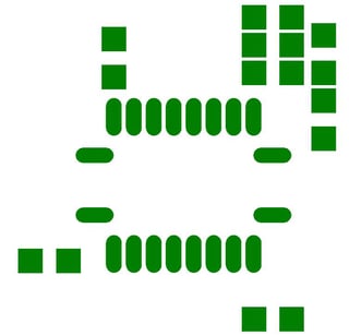
In flexible PCB designs with higher density SMT & PTH features and if the design allows, it is required to combine multiple feature openings into larger “ganged” openings to accommodate the above items.


Data as Supplied Revised Gang Opening Configuration
Coverlay/Flex LPI Design Combinations
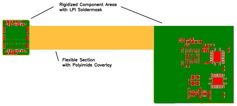
Some flex circuit designs due to their density, complexity, and/or component requirements may require the use of both materials. Both are selectively applied to specific areas of the part and provide benefits of both materials within one design. The manufacturing files are created to ensure that the two materials overlap within the rigidized area(s). This results in a complete encapsulation of the circuitry without the creation of mechanical bend stress concentrators in the flexible areas. If this were allowed the reliability of the part may be compromised. While this methodology adds some cost, the design may mandate it and/or the benefits outweigh the added cost.
Two common solder mask design configurations are to either apply flex LPI in rigidized component areas and polyimide coverlay in the flexible sections or to add selective webs of solder mask in ganged coverlay openings.
Example:

Additional Considerations
Designs that have one or more of the following may require the use of coverlay throughout in specific areas or layers:
- ZIF finger area Polyimide stiffener(s)
- FR4 component area rigidizing stiffener(s)
- Silver Ink Shield Layer(s)
- EMI & RF Shielding film(s)
- Pressure Sensitive Adhesives (PSA)
The materials above may not sufficiently adhere to LPI and pass IPC quality control requirements.
Key Takeaways
- Polyimide Coverlay Is the Industry Standard: It offers superior durability, flexibility, and dielectric properties compared to flexible LPI solder mask, making it the preferred choice for most flex circuit applications.
- Construction Impacts Performance: Coverlay is a two-part material (polyimide film + epoxy or acrylic adhesive) with common thicknesses of 1 mil film and 1 mil adhesive, selected based on bend radius, copper weight, cost, and encapsulation needs.
- Feature Machining Requires Extra Care: Openings for SMT and PTH features in coverlay are created using drilling, routing, or laser cutting, requiring larger annular rings, thicker webs, and the avoidance of isolated “island” features for reliability.
- Hybrid Designs Improve Reliability: High-density or complex flex circuits may combine polyimide coverlay in flexible areas with LPI solder mask in rigidized regions to balance durability, encapsulation, and assembly needs.
- Additional Design Considerations: Applications involving ZIF fingers, stiffeners, silver ink shields, EMI/RF shielding, or PSAs often require polyimide coverlay in specific areas, as these materials may not adhere well to LPI.


