


Dynamic flexible circuit boards are designed for applications that require continuous or repetitive motion while maintaining reliable electrical interconnections in a compact form factor. Successful dynamic flex circuit design depends on controlling bend radius, selecting the proper copper type, minimizing layer count, and managing shielding requirements to prevent premature circuit failure.
Dynamic Flexible Circuit Board Design Challenges
Dynamic flexible circuit boards solve interconnect and packaging challenges in applications that experience repeated movement. They support high-density interconnections while occupying minimal space, making them suitable for designs where traditional interconnect methods are not practical.
Unlike static or bend-to-fit flex circuits, dynamic applications require specialized design rules. Repeated bending places ongoing mechanical stress on the copper circuitry. If the copper is stressed beyond its ductility limits, it begins to work harden, lose flexibility, and eventually develop cracks that can result in open circuits and reliability failures.
Common dynamic flex applications include:
- Print head interconnects
- Rotating scanning assemblies
- Flip-up display interconnects
- Rotating actuators
- Linear actuators

Minimum Bend Radius Requirements
Why Bend Radius Matters
Bend radius is one of the most important design considerations in a dynamic flexible circuit. Proper bend radius selection helps ensure that copper conductors remain within their ductility limits throughout repeated flexing cycles.
The general guideline for dynamic flex applications is a minimum bend radius equal to 100 times the finished thickness of the circuit in the dynamic flex area.
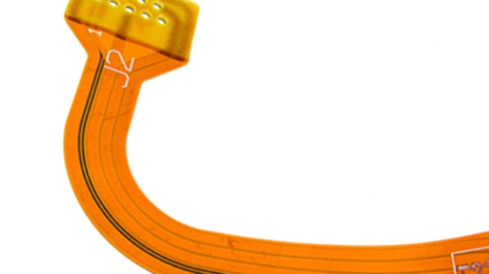
Flexible PCB is manufactured with the proper bend radius.
Bend Radius Example
For example, a flex circuit with a finished thickness of 0.005 inches requires a minimum bend radius of 0.500 inches, which corresponds to a minimum bend diameter of 1.000 inch for long-term reliability over an infinite number of cycles.
- Bend radius multiplier = 0.005 inches
- Minimum bend radius = 0.500 inches
- Minimum bend diameter = 1.000 inches
Material Selection and Bend Performance
The required bend radius can be influenced by material selection. Using thinner copper, thinner core materials, and thinner coverlay constructions can improve bend radius capability. However, these material choices may increase overall design cost.
Some flexible circuit designs contain both static and dynamic flex areas. In these cases, the design requirements for each area differ and should be evaluated separately.
Copper Options for Flexible Circuits
Two copper types are available for flexible circuit board construction:
- Electro-deposited (ED) copper
- Rolled annealed (RA) copper
Why RA Copper Is Preferred for Dynamic Flex
RA copper begins as ED copper and is then processed through a rolled annealed manufacturing process. This transforms the grain structure from the vertical orientation associated with ED copper into an elongated horizontal grain structure.
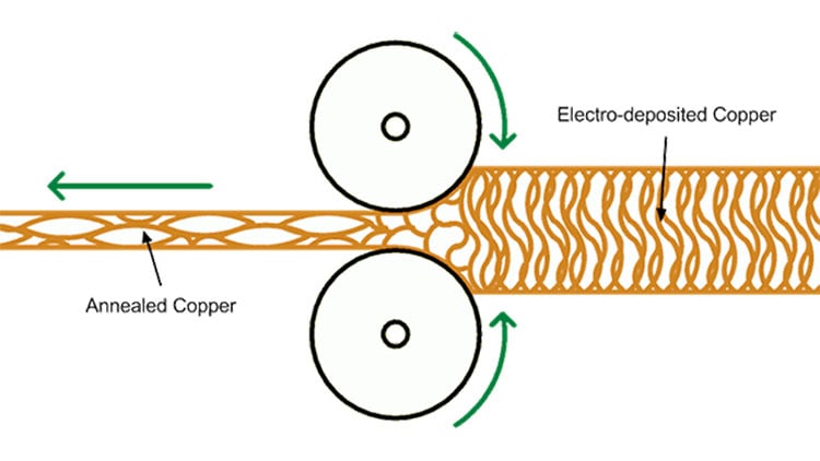
Example of copper being subjected to the rolled annealed process.
The resulting increase in ductility allows the copper to better withstand the effects of work hardening during repeated bending cycles. It also helps reduce the likelihood of micro-crack formation in the vertical axis.
Because the rolling process creates a grain direction, proper orientation is important in dynamic flex applications.
RA Copper Grain Direction Requirements and Availability
For dynamic flexible circuits, RA copper should be oriented, so the grain direction runs along the length of the flex circuit. Aligning the grain structure with the direction of bending provides the highest level of ductility and improves long-term flex performance.
RA copper is available in thicknesses ranging from:
- ¼ ounce
- 2 ounces
The most commonly used thicknesses are:
- ½ ounce
- 1 ounce
Layer Count, Neutral Bend Axis, and Layout Considerations
IPC 2223 Recommendations for Dynamic Flex
According to IPC 2223 design recommendations, layer count should be minimized in dynamic flex circuit applications because additional layers increase mechanical stress during bending.
One-Layer Construction
A one-layer construction is considered the optimum configuration for dynamic flex applications.
In a single-layer design, the copper circuitry is positioned at the center of the construction, referred to as the neutral bend axis. Locating the conductors at the neutral bend axis minimizes both compressive and tensile forces during flexing and provides the best long-term reliability.
Two-Layer Construction
A two-layer construction can be used when a thin adhesive-less flex core of 0.001 inch or less separates the layers.
This approach minimizes the distance between the circuitry and the neutral bend axis, reducing stresses generated during repeated bending.
Additional layout recommendations for two-layer dynamic flex designs include:
- Avoid solid fills
- Avoid cross-hatched fills
- Stagger traces from layer to layer
- Minimize the I-beam effect
Three-Layer and Higher Constructions
Three-layer and greater constructions are generally not recommended for dynamic flex applications. When these designs are used, bend radii substantially greater than 100 times the finished thickness may be required.
EMI and RF Shielding for Dynamic Flex Circuits
Preferred Shielding Method
When EMI or RF shielding is required in a dynamic flexible circuit, shielding films are the preferred solution.
Using copper layers or silver ink for shielding increases circuit thickness and reduces bend capability. In contrast, shielding films provide effective shielding performance while preserving flexibility.
Shielding Film Characteristics
Shielding films offer several advantages:
- Effective EMI and RF shielding
- Thin construction of approximately 17–22 um
- High flexibility
- Compatibility with one- and two-layer flex circuits
- Installation on one or both sides of the circuit
Grounding and Interconnection
Shielding films use electrically conductive adhesive to connect to a ground circuit through selective openings in the coverlay.
In two-layer designs, non-plated holes can be used to electrically interconnect shield layers on opposite sides of the circuit.
Key Design Considerations for Reliable Dynamic Flex Circuits
Successful dynamic flex circuit performance depends on applying the appropriate design rules and material selections throughout the design process.
Key considerations include:
- Maintain a minimum bend radius of 100 times the finished thickness.
- Use RA copper rather than ED copper for dynamic applications.
- Orient RA copper grain direction along the length of the flex circuit.
- Keep layer counts as low as possible.
- Position circuitry near the neutral bend axis.
- Avoid solid and cross-hatched fills in two-layer constructions.
- Stagger traces to reduce stress concentrations.
- Use shielding films instead of copper or silver shielding layers when EMI or RF protection is required.

Summary
Dynamic flex circuit applications solve a very wide variety of packaging challenges and create design opportunities that no other interconnect method can provide. Following the recommended design rules and material selection will ensure a successful and reliable design.
Key Takeaways
- Minimum bend radius is critical: Dynamic flex circuits require a bend radius of at least 100 times the finished thickness to prevent copper from hardening and cracking over repeated cycles.
- Rolled annealed copper is required: RA copper, with its horizontal elongated grain structure, offers superior ductility and must be oriented correctly along the bend direction to withstand repeated motion.
- Layer count must be minimized: One-layer designs are optimal since they place copper traces at the neutral bend axis. Two-layer designs may be used with very thin cores, but three or more layers are discouraged due to excessive stress.
- Layout techniques improve reliability: Avoiding solid fills, staggering traces between layers, and maintaining proper placement relative to the neutral axis help reduce stress concentrations and extend flexible circuit board life.
- Shielding requires thin films, not copper layers: For EMI and RF needs, shielding films with conductive adhesives are preferred, as they maintain flexibility without adding significant thickness or restricting the bend capability.


