Many electronics assemblies that utilize flexible printed circuit boards are sensitive to either absorbing or emitting electromagnetic interference (EMI). If EMI is left uncontrolled it can negatively impact the performance of the design and in extreme cases completely prevent it from functioning.
The method to address this interference is to “shield” the circuitry to prevent EMI from being either absorbed or radiated. For many applications there are industry standards that apply to regulation of the radiation of EMI from a design established by the FCC, IEC, EU etc.
EMI Shielding Requirements in Common Applications
Below are some of the common applications in the medical, communications, and military industries that often require EMI shielding.
Medical Systems:
- MRIs
- Infusion pumps
- Patient monitoring systems
Communications Systems:
- Cell phones
- RF communications
Military Systems:
- Radar systems
- Communication systems
- High-speed data transmission designs
PCB Shielding Method
Shielding a design requires that it be encapsulated on both sides with a layer of material that acts as a barrier to the absorption or radiation of EMI. These layers are connected to ground so that any EMI is harmlessly dissipated.
There are additional considerations that must be factored in when choosing a shield method and material.
Bend Requirements
Each shielding method adds different amounts to the overall thickness of the flexible circuit. As the minimum bend capability is a function of the thickness, it will reduce or limit the bend capabilities of a design. The minimum bend radius and type of bend requirement of shielded designs needs to be accurately defined and reviewed as part of the design and material selection process.
The type of bend requirement, either static (bend once to fit) or dynamic (repetitive bending), places further constraints. A dynamic bend flex PCB application has a much larger minimum bend capability than that of a static bend design.
Controlled Impedance
Controlled impedance signal requirements place further limitations on the shielding method that can be used. The shield(s) require electrical characteristics that satisfy both the EMI requirements as well as perform as reference planes to achieve the required controlled impedance values. Not all shielding methods can satisfy both.
Shielding Materials
There are primarily three types of shielding materials used in the industry. Each has positives and negatives in terms of shielding performance, impact on mechanical bend capabilities, and suitability for controlled impedance designs.
Silver Ink Shields
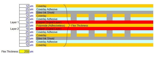
Silver ink shields consist of added layers of silver conductive ink which are selectively applied to the coverlay surface that encapsulates the circuit patterns. Coverlays have selective openings which are stitched along outside edges of the length of the part which exposes the ground circuit of the design.
The ink flows into the selective openings, adhering and electrically connecting to the ground. Silver ink is most commonly applied using a silk screening method. This method can limit the accuracy and location of the shield. Additional layers of coverlay are then laminated to the silver ink layers to encapsulate and electrically isolate them.

Example of a 2-layer flex PCB construction with silver ink shields.
Silver Conductive Ink Advantages:
- Cost effective
- Good flexibility
- Good shielding capability
Disadvantages:
- Not suitable for controlled impedance designs
- Requires multiple coverlays (added materials & process steps)
- Reduced demand in industry
Copper Layer Shields
Copper layer shields consist of additional etched copper layers added externally to the construction, increasing the design layer count. Copper layers can either be solid planes or crosshatched for improved flexibility but with reduced shielding capability. They require additional vias in the flexible area(s) if ground stitching is required.

Example of a 3-layer flex PCB with copper shields.
Copper Layer Advantages:
- Highest degree of shielding
- Solution for controlled impedance designs
Disadvantages:
- Most expensive solution
- Greatest negative impact on flexibility
- Stitched vias can further negatively impact flexibility by created mechanical bend stress concentrators
Shielding Films
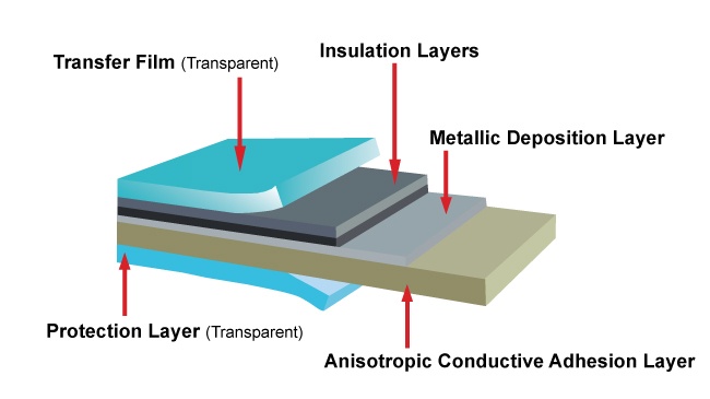
Shielding film consists of an additional layer of selectively specialized laminate on the surface of the coverlays. These films were developed to meet the requirements of the cell phone/digital camera and camcorder markets. As with silver ink, selective openings in the coverlay expose the ground circuit and create interconnect locations. The shielding films have a 3-layer construction consisting of an electrically conductive adhesive, a metallic deposition layer and an isolation layer.

Example of cross section structure of EMI shielding film.
The isolation layer is black in color as well as friction resistant. The films are laminated under heat and pressure. The conductive adhesive flows into the coverlay opening which then adhere and electrically connect to the ground.

Example of a 2-layer flex PCB with shield film layers.
Shielding Film Advantages:
- Best Flexibility
- Thinnest Overall Construction
- Cost Effective
- High Degree of Shielding Capability
- Increasing Popularity
Disadvantages:
- Limited Applications for Controlled Impedance Designs
Summary
For many flex PCB designs, EMI shielding is a critical element that ensures the overall performance of the final product. The variety of available shielding methods and material options allow for effective designs which enable all electrical and mechanical requirements to be achieved.
Key Takeaways
- EMI shielding is essential for performance and regulatory compliance: Many medical, military, and communication applications require shielding to meet FCC, IEC, or EU EMI regulations and ensure reliable operation.
- Each shielding method impacts flexibility and impedance differently: Silver ink, copper layers, and shielding films all offer varying trade-offs between shielding effectiveness, cost, bend radius, and suitability for controlled impedance designs.
- Shielding films offer the best flexibility and are gaining popularity: These films are ideal for space-constrained applications with dynamic bending and offer good EMI protection, though they’re not ideal for impedance-sensitive designs.
- Copper layers provide the highest EMI protection and impedance control: Best for high-performance applications requiring strict signal integrity, but they increase cost and reduce flexibility significantly.
- Designing for EMI requires early planning of mechanical and electrical factors: Bend requirements (static vs. dynamic), layer thickness, ground connections, and impedance goals must all be considered when selecting the right shielding method.


