


The flex PCB stack-up documentation is an important component of the data set of a flexible printed circuit board design. It consists of a description of a flex or rigid-flex circuit board that defines in detail the specific material requirements and construction of the design.
The material stack-up is required by the supplier to ensure that the finished part is manufactured according to all customer specifications and meets both the mechanical bend requirements and electrical requirements of the design.
Material Stack-up Format
Flex PCB material stack-ups are a graphical, side view profile of the flexible printed circuit board which is typically embedded in the mechanical drawing in either PDF, DXF, or Gerber format.

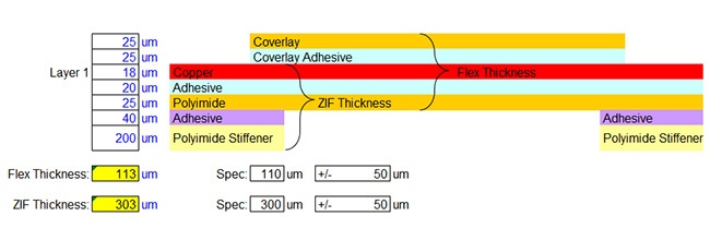
Example of a 2-Layer Flex Circuit Stack-up with ZIF Contacts
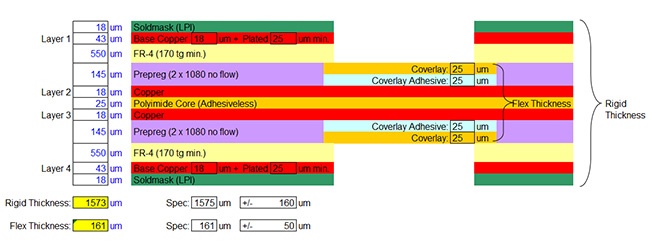
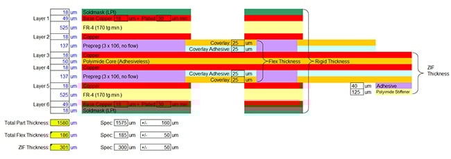
Example of a 4-Layer Rigid-Flex Circuit Stack-up
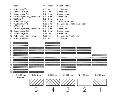
Stack-up Material Information
As seen in the previous examples, the stack-up contains a significant amount of information. It defines the specific material types to be used, their locations within the construction, the individual material layer thicknesses, material part numbers if required, and the total thickness of the various areas of the design.
Most flex and rigid-flex circuit designs have multiple areas with differing constructions resulting in multiple thickness requirements. Some area thicknesses may be critical to the performance of the part, either to meet a specific bend requirement, impedance value, or connector specification (ZIF connectors, for example).
For rigid-flex PCB designs, the stack-up also defines the key construction elements required to meet IPC 2223C design guidelines and ensure the reliability of the finished parts.
Specific elements include:
- Adhesiveless flex core(s)
- Selective coverlays applied to the exposed flex areas only and not within the rigid areas
- No-flow pre-preg for rigid layer lamination and high TG FR4 rigid cores
Common Material Details
Along with the material stack-up information, below are some additional details that should also be included.
Flex Cores:
- Type (Adhesive or Adhesiveless)
- Thickness, Copper weights
- Copper Type (ED or RA)
- Lamination Adhesive Thickness
Coverlays / Soldermask:
- Thickness
- Adhesive Thickness
- Adhesive Type (Epoxy, Acrylic etc.)
- Color
Stiffeners:
- Material Type (FR4, Polyimide, Aluminum, Stainless etc.)
- Thickness
- Attachment Adhesive (PSA or thermally bonded)
Additional Materials:
- PSA (Pressure Sensitive Adhesive)
- EMI Shielding Films
- Epoxy Strain Reliefs
Flexible circuit board designs typically have a finished thickness tolerance of +/- 30um to 50um or larger depending upon the layer count. The thickness of a flex circuit will vary depending upon where the part is measured. It will also vary due to the adhesives having a reduced thickness after lamination due to a percentage of the material being consumed by filling in the spaces between traces.
Complex Flex and Rigid-Flex PCB Designs
Complex flex designs that have multiple extensions may require the material stack-up to be divided into regions to allow for a full and clearly defined description of the design. Trying to define the part in one stack-up results in areas of differing construction overlapping and distorting the graphical representation of the design. The specific regions are then identified in the part outline.
Example of Advanced Multiple Area Material Stackup
Example of Flex Circuit Drawing with Multiple Area Material Stack-up
Example of Advanced Rigid-Flex Circuit Material Stack-up
Flex Board Material Specifications
We recommend that the flexible and rigid materials (if required) be defined by IPC standards as part of the drawing notes. This allows for the use of equivalent material brands that meet the same IPC specifications. It’s not practical for a supplier to stock all the available material brands and configurations. In addition, not all material brands are readily available or cost effective in different geographical areas.
The exception to using these specification standards is for designs that require specialty materials for which there are no existing IPC standards or have specific performance requirements. This most commonly applies to high performance flex materials, PSAs, shielding films, and epoxy strain reliefs. If known equivalents are available, the drawing notes should state “or equivalent”.
Examples of specialty materials:
- PSA(s): 3M9077, 3M467MP, etc.
- EMI Shielding Films: Tatsuta SF-PC6000
- Flex materials: DuPont TK, DuPont HT
- Epoxy Strain Relief: Eccobond 45/15 Flexible Formula

Summary
All flex or rigid-flex PCB designs require a complete and accurate PCB stack-up as part of their included documentation to ensure the supplied parts meet all the design requirements for the customer. Ensuring that this information is correct helps eliminate unnecessary technical questions from popping up and avoiding delays in the delivery time of your parts.
Watch Our Video:
Designing Flex and Rigid Flex PCB Stack-Ups with Advanced Software
See our in-depth tutorial on creating a stack-up using our advanced software! In this video, we walk you through the process of generating a new stack-up, starting with the default settings and customizing it to fit your specific requirements.
Key Takeaways
- Stack-Up Drawings Are Essential for Accurate Manufacturing: A flex or rigid-flex PCB stack-up shows the side-view construction, material types, layer thicknesses, and special requirements, ensuring the final product meets both electrical and mechanical performance specs.
- Multiple Construction Zones Require Regional Stack-Ups: Complex flex and rigid-flex boards with different material needs in various areas should be defined in regional stack-ups to avoid confusion and maintain clear, manufacturable documentation.
- Include Specific Material and Thickness Details: Key details like flex core type, copper weight and type, coverlay thickness, stiffener material, and adhesives should all be clearly defined to reduce manufacturing ambiguity and maintain performance.
- Use IPC Standards Whenever Possible: To ensure material availability and cost-efficiency, designs should reference IPC material specifications unless proprietary or specialty materials are required for high-performance or niche applications.
- Expect Thickness Variations and Tolerances: Flex circuits naturally have ±30μm to 50μm tolerance ranges, especially due to adhesives compressing during lamination and varying trace layouts, so design requirements should account for those variances.


