It is critical for any flex circuit design to be free of errors and violations in order to get the application to market as fast as possible without unnecessary delay. To help designers avoid common IPC PCB design standards violations in rigid-flex PCBs, this blog post will discuss three of the most common IPC Association Connecting Electronics Industries design violations.
Callout Appropriate Flex Core Material
In order to meet IPC design standard 2223C, the design must callout for a flex core that is adhesiveless. There are two types of materials that are used throughout the flex industry and they differ as to how the copper is attached to the core.
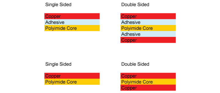
Example of Flexible Circuit Material Constructions

Older generation material known as “adhesive based” consists of a layer of adhesive which is used to bond the external copper with the flex core creating a sandwich effect. A two-layer construction would consist of copper, layer of adhesive, layer of polyimide, another layer of adhesive, and the last layer of copper. The newer generation material is referred to as being adhesiveless. With this material the copper is attached directly to the polyimide core, there is no adhesive. Visually it would appear as copper, polyimide, copper.
The reason why the new material meets the rigid flex PCB design standard versus the older material is because the adhesive has a very high coefficient of thermal expansion. If you take an adhesive based core and drill the vias through the rigid sections they also pass through the flex core. During the assembly process and operation of the finished part afterwards, the adhesive will expand and contract as the part heats up and cools down. This places a lot of stress on the plating of the vias to the point where the copper in the vias will start to work harden, becomes brittle, and it eventually cracks. The result of this causes an intermittent open. Sometimes the circuit will separate enough to create a complete open and at other times it could contract, creating a connection.
In the late 90’s and early 00’s, as designs became more complex, the industry as a whole began to recognize that there was an increase in intermittent cracked via opens. It was determined that the issue was a direct result of the adhesive in the older generation flex core. This ultimately led to the development of adhesiveless material which is proven to eliminate the issue.
Polyimide Coverlay Application
Polyimide coverlays are laminated onto the surface of the flex layers to encapsulate the circuitry and serve the same purpose as solder masks do to rigid boards. The coverlay is laminated to the flex circuit with the same adhesive used in the older generation material.
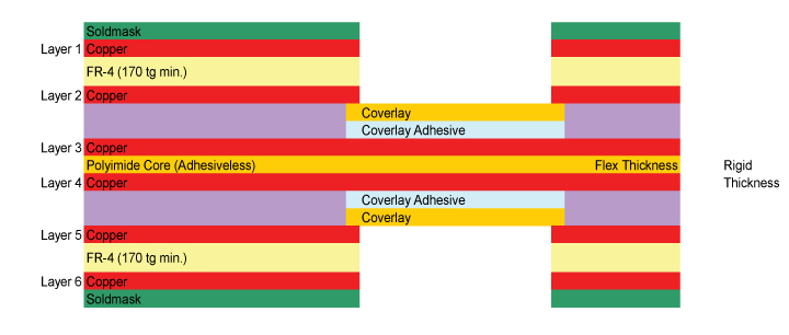
Example of a Flexible Circuit Selective Coverlay Construction
There are some older construction methods where the coverlay is applied across the entire flex circuit layer which results in the coverlay being included within the rigid sections. This creates the identical issue of the high coefficient of thermal expansion leading to experiencing the encounter of cracking of vias.
The correct IPC approved method is to apply the coverlays selectively, (also referred to as a “Bikini build” construction) applying only to the exposed flexible areas of the design. This eliminates all adhesives from within the rigid area and prevents the formation of via or PTH plating cracks.
Via Locations
Issues arise when vias are located within a rigid section(s) closely adjacent to the line where the flex sections extend out from within the rigid areas.
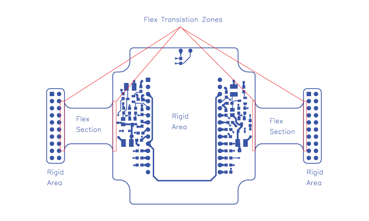
CAD Drawing of Via to Flex Transistion Location
The portion of the outline of the rigid section to where the flex section meets is known as the flex transition line. With the correct IPC Selective coverlay construction the coverlay does however have to engage into the rigid section by a small distance so that it can be trapped and it will have a full seal with no gaps or any discontinuities.
This distance is typically between .025” and .030”. It will vary slightly due to manufacturing and material tolerances.
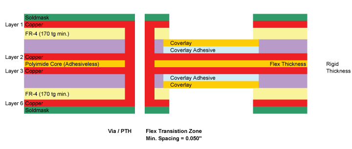
Another Example of Via to Flex Transistion Location
Vias have a keep out area in relation to the flex transition line. Designs should not have plated vias close to the transition line. Having a via or PTH too close could result in catching the coverlay and again creating a plating reliability issue. IPC recommends a minimum distance of between 0.050” and 0.100” where we suggest .050” from the edge of the plated through hole to the flex transition zone.
Interconnect Stress Testing
An accelerated reliability/performance assessment test was developed called the Interconnect Stress Test (IST) and incorporated into IPC TM-650 Test Methods. IST testing of a rigid flex circuit board design with any of the non-approved issues mentioned above will result in a failed test and is a strong indicator of both at assembly and long term reliability issues. Following IPC 2223C recommendations will ensure the highest degree of reliability.
Summary
The best opportunity for success is for both the manufacturer and customer to work together as early as possible in the design phase. At this stage we can assist in evaluating the mechanical configuration of the circuit board design, where the flex areas will be located, and the layer count(s) required. We can then provide a preliminary stack-up which will specifically identify to the customer the adhesiveless flex core, the selective flex only area coverlay, and graphically define restricted areas for via / PTH placement that are adjacent to the flex transition zone. Having done all this, the process is often streamlined without major complications. All flex and rigid-flex designs are carefully created to avoid violations that do not meet IPC PCB design standards.
Key Takeaways
- Adhesiveless Flex Cores Are Required: IPC 2223C mandates adhesiveless flex cores, as adhesive-based materials expand and contract under heat, leading to cracked vias and intermittent opens.
- Adhesive Expansion Causes Reliability Issues: Older adhesive-based cores were directly tied to via failures, which drove the industry to adopt adhesiveless materials for improved long-term reliability.
- Selective Coverlay Application is Critical: Coverlays must only be applied to exposed flexible areas (“bikini build”), keeping adhesives out of rigid zones to avoid plating cracks.
- Via Placement Rules Near Flex Transition – Vias should not be located too close to the flex-to-rigid transition line; IPC recommends keeping plated vias at least 0.050” to 0.100” away.
- Interconnect Stress Testing Ensures Reliability: IPC’s IST testing quickly identifies non-compliant constructions, reinforcing the need to follow IPC 2223C for manufacturable and reliable flex designs.


