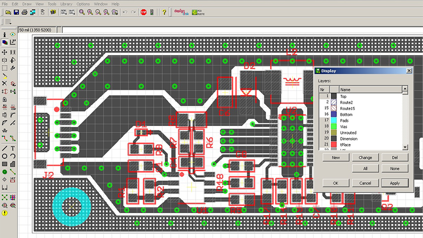
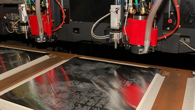
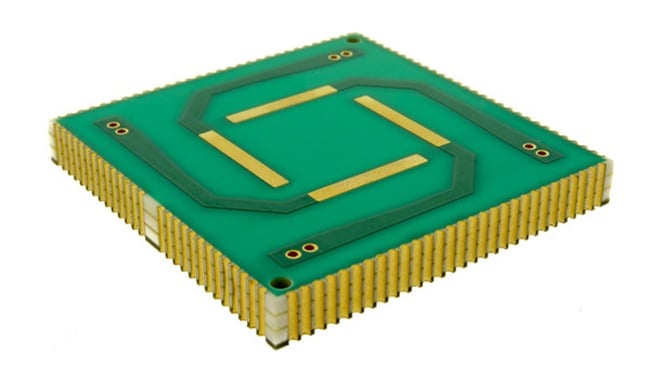
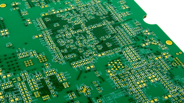
It is sometimes necessary to have some, or all, of your PCB layout projects done by an outside source. If you’ve never done a layout before, or if you don’t have the tools or experience to take on more complex projects, it is often better to have a professional complete the work.
Read MoreAl Wright

Recent Posts
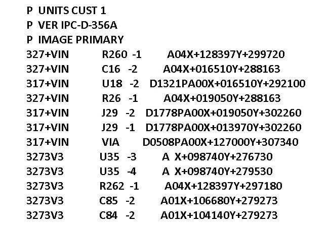
Nobody wants to experience the feeling of populating your new printed circuit board (PCB) design and finding out that it is not electrically functional. Most often, the lack of functionality is attributable to a specific production problem or a combination of several different problems. Sometimes, however, the problem is that the Gerber files exported from your PCB CAD program contained an error that went unnoticed because there was no way to verify that the files matched your design intent. You can avoid a good deal of trouble by supplying an IPC-356 format netlist file with your fabrication data package.
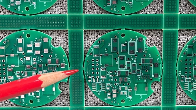
Read MorePrinted circuit board (PCB) designers often find themselves at odds with their purchasing and marketing departments after a design goes out for bids and comes back with a larger than expected price tag. Once the source of the high cost is identified, the questions fly, the fingers point, and the nerves fray.
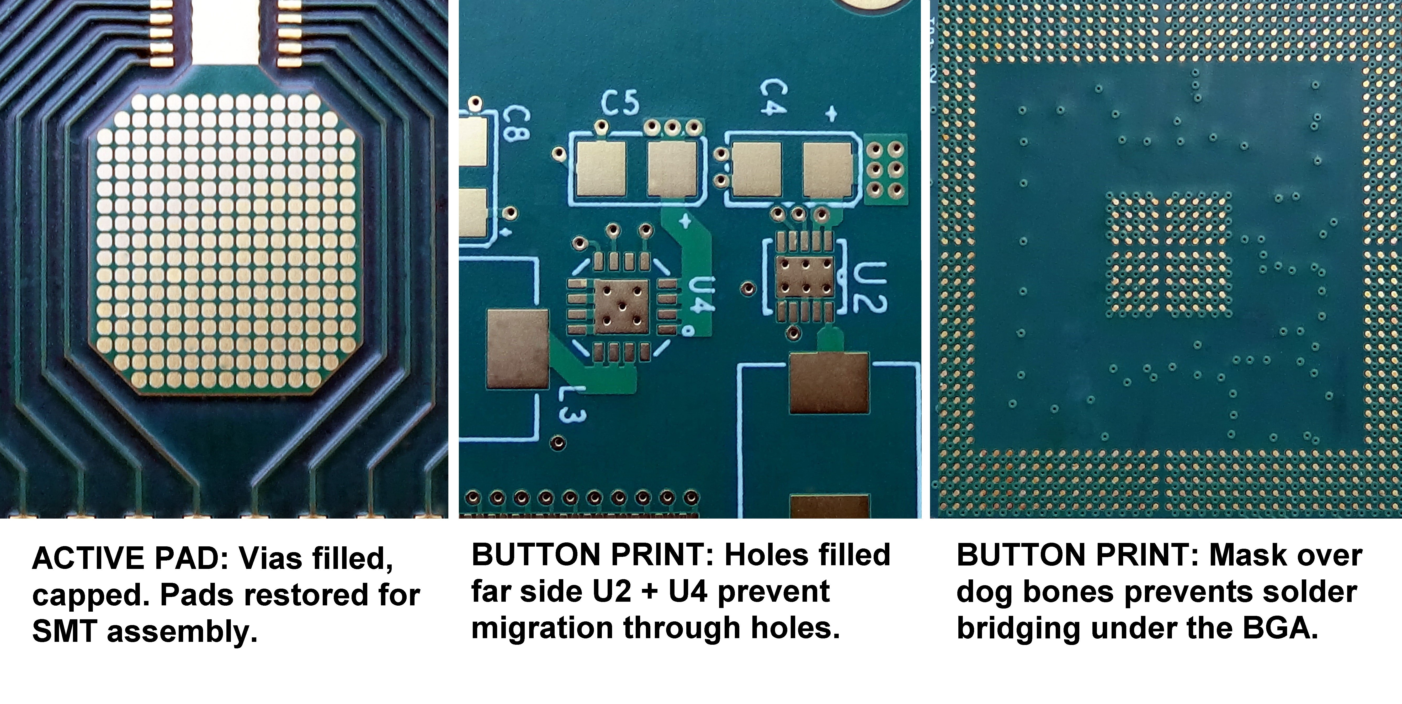
Read MoreAs today’s printed circuit boards (PCBs) become smaller, they use fewer and fewer through hole components. It is increasingly difficult to justify allocating precious space for relatively large plated through component holes and their accompanying lands. Instead, it is necessary to use surface mounted components wherever possible. As surface mount technology becomes increasingly prevalent, the majority of the plated through holes on most modern PCB designs end up being vias.
Read MoreAmong the most common questions printed circuit board suppliers receive are those dealing with production capabilities. Customers often suspect that they are about to design-in a feature which may be either at or outside their fabricator’s limits. Fearing that their non-standard feature may add cost to their product, they inquire to find out just how much pain they are about to cause.
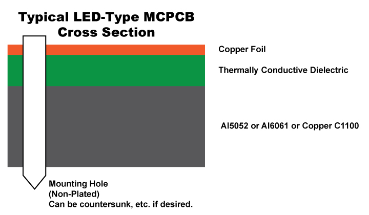
Read MoreOver the past several years LED based products have become increasingly popular, and as a result, so too have metal core printed circuit boards. The automobile and lighting sectors have both embraced the technology, as have consumers, given an LED based light can be about 5x cheaper to run than a comparable incandescent unit. Even compact fluorescents have slightly higher operating costs, and they cannot compete with the smallest LEDs when it comes to efficient use of space.
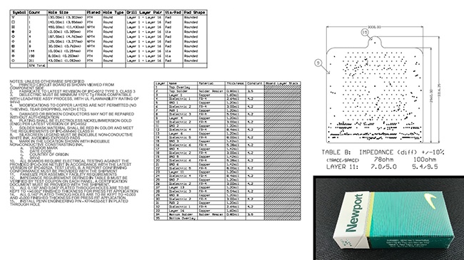
Read MorePrinted circuit board (PCB) fabricators receive dozens of requests for quotations (RFQs) every day. While many requests have moved to more convenient online quoting formats such as our in-house application InstantPCBQuote, many customers still send requests the old way via either files or alternate forms of describing their manufacturing requirements.
Read MoreSelecting PCB core thickness becomes a problem when a printed circuit board (PCB) fabricator receives a request for quotation of a multilayer design and the material requirements are stated either incompletely or not at all. This sometimes occurs because the combination of PCB core materials used is not critical to performance; if the overall thickness requirement is met, the end user may not care about the thickness or type of each layer.
Read MoreAll customers have questions when it comes to PCB laminate materials, so we took some of the most common questions and put together a helpful FAQ to bring you answers and solutions faster.
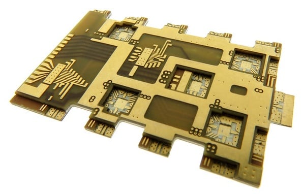
Read MoreIf you’re a designer of RF or microwave printed circuit boards you’ve probably already selected a laminate material that is appropriate to your project, having based your choice primarily on the electrical requirements of the circuit, such as signal speed, loss rate etc. Be careful, however, not to overlook the fact that the specialty materials used in such designs also possess unusual mechanical characteristics; processing is different from that of normal FR4 boards.
Read More


