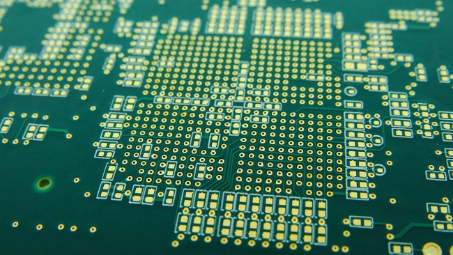
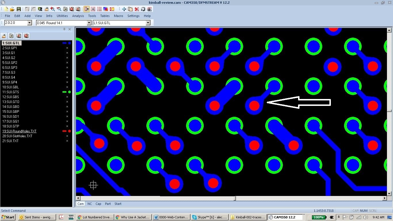
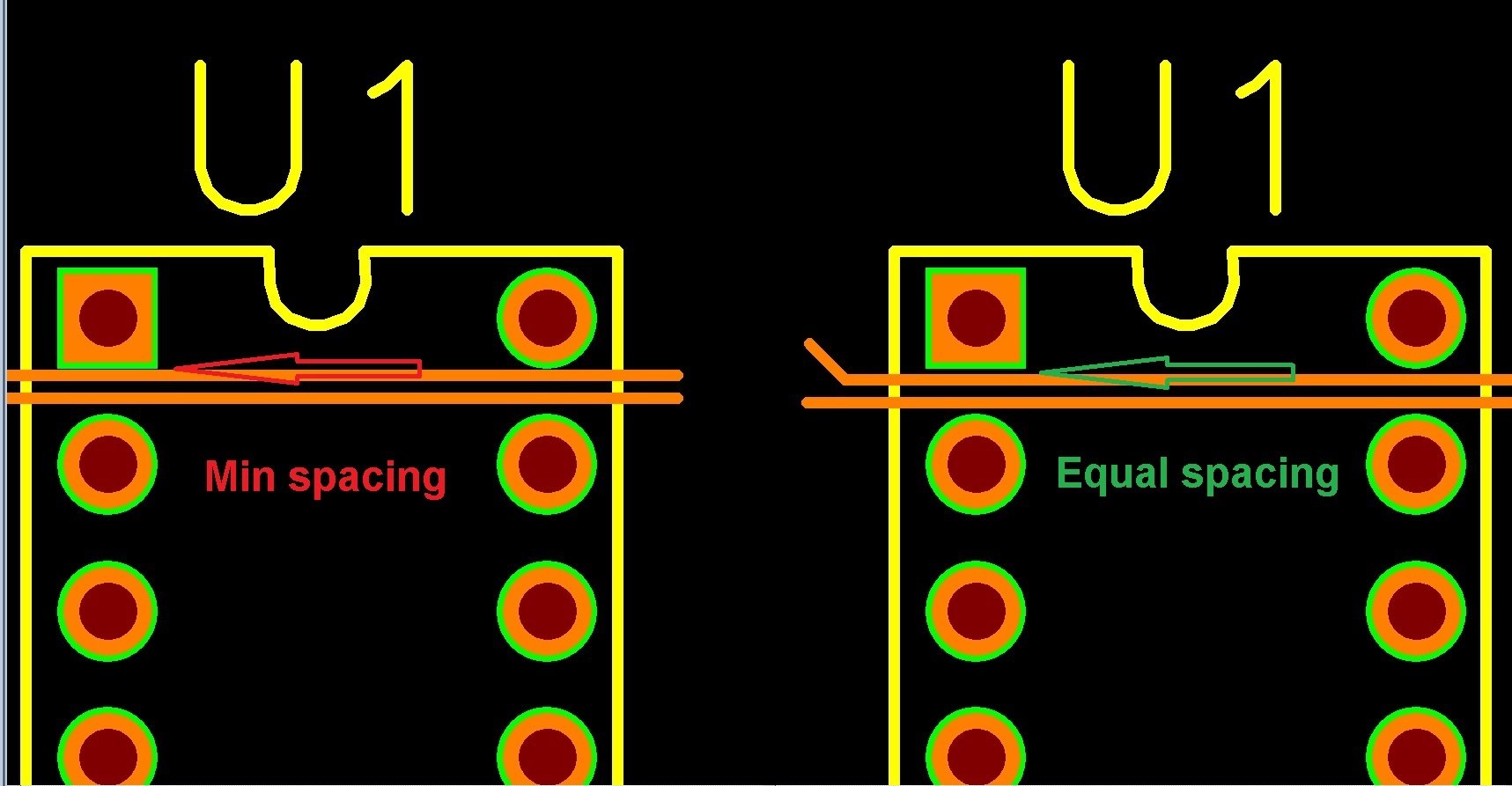
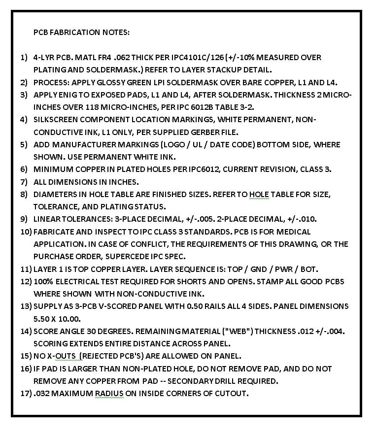
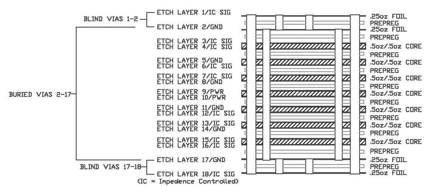
Miniaturization in electronics drives the need for both component and printed circuit board designers to work within ever-shrinking footprints in order to remain competitive. The signal routing requirements for many ball grid array (BGA) components are such that through hole via drilling is becoming less and less practical. This makes it necessary in many instances to use blind vias to form interconnections between layer pairs.
Read MoreAl Wright

Recent Posts
Printed circuit boards (PCBs) continue to shrink. As each generation of miniaturized components comes along, board designers find themselves able to work within ever-smaller PCB footprint sizes. While this is great news for consumers (compare the size of a 1994 portable phone to one of today’s models) it presents difficulties for fabricators.
Read MoreAs printed circuit board (PCB) designs have increased in complexity, they have both decreased in size and increased in density. Physical changed to circuit boards have forced PCB designers and manufacturers to develop new PCB layout strategies aimed at making full use of all available surface area.
Read MoreWhen placing an order or requesting a quotation for printed circuit boards (PCB), it is extremely important to clearly state all of your requirements as completely as possible.
While this may seem obvious, it is surprisingly common for PCB fabricators to submit a pricing estimate to the customer based on information supplied within the request for quotation, only to receive additional information after pricing and delivery have already been agreed upon and a purchase order issued. If the new information affects the price and/or lead time, the fabricator must notify the customer of the changes in terms.
Read MoreYour PCB design for manufacturing is critical to the success of your final application. Design features which make your board difficult to build add cost to your product, either by slowing down the production process, or by increasing the scrap rate.
Read MorePCB Laminate Utilization - Part and Panel Size:
In our first post on controlling PCB costs, we detailed many of the common cost drivers people face and ways to avoid them. For part 2 of controlling costs, we are focusing on one example that can cost a lot of dollars: PCB laminate costs and utilization
Printed circuit boards are run through the fabrication process in sheet form, typically with rows and columns of identical circuit boards or sub-panels on a single sheet, which are later cut out for shipment. One of the biggest potential cost adders in PCB manufacturing is that of a poor-yielding PCB or sub-panel. While this is true for even the least complex PCBs, it is especially true for multilayers.
Read MoreAvoiding Expensive PCB Materials & Processes
Printed circuit boards are only one component of an entire assembly designed to meet the best cost-to-performance ratio possible. The finished product into which the PCB is installed must meet a price point that compares favorably against competing products, so the lower the expenses, the more money your product returns. In order to make the best choices during the design cycle, it is important to first understand what drives the primary costs.
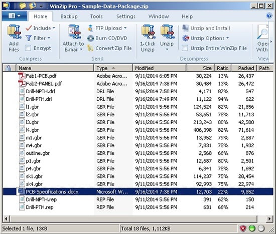
Read MoreIn order for Epec or any PCB fabrication company to quote your circuit boards accurately and with minimum delays, it's important to supply a complete PCB data file set, using industry-standard file types. Before you look at getting your quote, learn what information you need to supply to ensure a smooth PCB fabrication process.
Read MoreWave soldering, the process of attaching electronic components to the printed circuit board (PCB), becomes increasingly difficult as pitch decreases. Pitch is the center-to-center spacing between the conductors on a PCB. So, knowing that wave soldering becomes harder with lower pitch measurements, what is the minimum pitch distance you should maintain on circuit boards? With the appropriate controls, it is still possible to get a good result with pitches as low as 0.5mm (.0197"). Wave soldering defects can occur in pitches below 0.5mm, so we recommend this as the minimum pitch to wave solder a PCB.
Read MoreWhen it comes to printed circuit board manufacturing, there are a variety of PCB via process requirements to consider. Each has their own pros, cons, and cost adders so knowing these requirements can aid you when designing your circuit boards. In this post we will discuss the differences for why you would either fill or plug a circuit board via.
Read More


