


When it comes to printed circuit board manufacturing, there are a variety of PCB via process requirements to consider. Each has their own pros, cons, and cost adders so knowing these requirements can aid you when designing your circuit boards. In this post we will discuss the differences for why you would either fill or plug a circuit board via.
Filled Vias
Non-planar filling (without over-plating) prevents solder from migrating away from a nearby surface mount pad and down through the via during the PCB assembly process. It also helps to form a vacuum for assembly and for electrical testing.
Partially filling the barrel compensates for an LPI solder mask's inability to form a true 100% "tent" across the via, as dry film masks were able to do in the past.

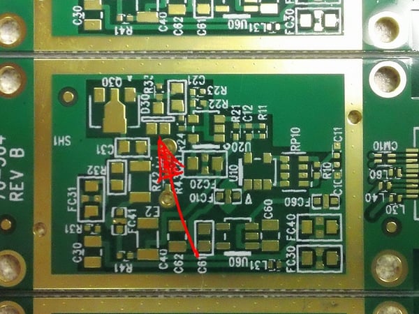
Printed Circuit Board Surface Mount Pad After Via Pad Process
Plugged Vias
Plugging (with planarization and over-plating) is alternate option. If vias must be drilled through component mounting pads on a high density PCB, the plugs can be drawn down to completely fill the vias. The surface is then planarized and plated over, so that the pads can be used for soldering.
The over-plating option adds cost but some of that cost can be recovered through the use of smaller circuit board footprints and reduced layer count.
Summary
When designing PCBs, the decision to fill or plug vias can have a direct impact on assembly performance, electrical reliability, and overall manufacturing cost. Filled vias prevent solder wicking, improve vacuum hold during testing, and compensate for solder mask limitations, while plugged vias with planarization and over-plating enable soldering directly over via-in-pad designs common in high-density circuit boards.
Although plugging adds cost, it can also reduce layer count and board size, offering trade-offs that may ultimately lower overall system costs. Understanding these options allows engineers to select the most efficient and reliable via process for their design requirements.
Key Takeaways
- Filled vias prevent solder migration during assembly, keeping solder on nearby surface mount pads instead of wicking into via barrels.
- Partial via filling supports solder mask performance, compensating for LPI masks that cannot fully tent vias.
- Plugged vias with planarization and over-plating allow via-in-pad designs, enabling soldering directly on top of vias.
- Via plugging adds manufacturing cost but can save money by reducing PCB footprint and overall layer count.
- Choosing the right via process depends on design needs, balancing reliability, assembly performance, and cost trade-offs.


