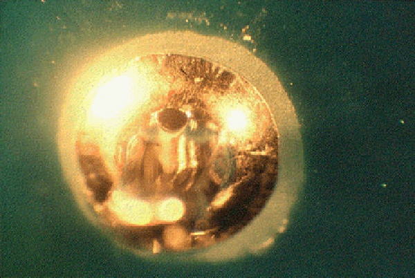
When a blow hole defect occurs during the assembly process as a result of the PCB card, the primary culprit tends to be entrapped moisture or air. With moisture, any non-plated and non-masked areas on a bare circuit board that expose internal laminate can be suspect to absorbing moisture. Absorption can occur either during the board fabrication process or from improper storage. Examples of highly suspect areas include non-plated drilled holes and routed features.

Blow Hole on Printed Circuit Board Magnified

Baking the circuit boards before assembly can help resolve these issues, although proper board storage is just as important. Bare PCBs should be stored in vacuum sealed bags with desiccant and humidity indicators. The packages should then be stored in areas devoid of high temperatures and high humidity.
In rare instances, boards can entrap air pockets behind plating. This is a process indicator for the PCB manufacturer. Rough drilling of plated through holes can lead to slight gaps between plating and the laminate within those holes. When the board is exposed to high temperatures during assembly, the entrapped air can expand rapidly and "blow" through thinner copper plating. This can be verified via micro-section of circuit board blow holes.
Explore our resources to learn more on wave soldering defects or additional PCB layout and design information.
Summary
Blow hole defects in PCBs typically result from entrapped moisture or air within the board. Moisture absorption can occur during fabrication or from improper storage, particularly in exposed areas such as non-plated holes or routed features. Proper storage practices, including vacuum-sealed packaging with desiccant, help minimize risk.
In rare cases, poor drilling or plating can trap air pockets that expand under heat during assembly, rupturing the copper plating. Identifying and addressing these root causes is critical to preventing blow hole failures.
Key Takeaways
- Moisture Absorption Is the Leading Cause: Exposed laminate areas like non-plated holes are prone to taking on moisture, which expands during assembly and causes blow holes.
- Proper Storage Is Essential: Vacuum-sealed packaging with desiccant and humidity indicators protects bare PCBs from moisture damage before assembly.
- Pre-Bake Prevents Failures: Baking boards before assembly drives out moisture and reduces the likelihood of blow hole defects.
- Entrapped Air Can Also Contribute: Poor drilling or plating processes may trap air pockets that expand during heating, rupturing copper plating.
- Defects Can Be Verified Through Testing: Micro-section analysis of defective boards helps confirm plating or drilling-related causes of blow holes.


