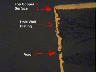
Selecting the optimal heavy copper thickness to apply to the plated through hole (PTH) plays a critical factor towards the overall reliability of the printed circuit board. There are two key elements to consider when determining optimal PCB copper thickness. The first is the current capacity of the barrel for acceptable heat rise. The second is the mechanical strength determined by the copper thickness, hole-size and whether or not there are any support vias.
Read MoreAl Wright

~ In Memoriam ~ Al was in the industry for more than 35 years, and 18 of those years were at Epec up until he passed away in December 2019. As field application engineer, he handled a wide range of responsibilities, including reviewing PCB designs for manufacturability during the quoting and design stage, interacting with off-site manufacturing facilities to solve technical issues during production, and programming CNC machines for in-house projects, reworks, and modifications. Al’s technical expertise was essential to Epec’s engineering department and provided valuable insight when working with customers. Prior to working at Epec, Al spent 20 years with CPC Incorporated, a medium-sized PCB manufacturer, learning hands-on about PCB processing before moving into front end engineering. Al brought a wealth of impressive expertise to Epec and worked with more than 50,000 different PCB designs from his start in 1981 through 2019. He worked with Epec’s team to get all designs right ahead of time so that products were correct the first time. Most recently, Al was instrumental in helping Epec establish its heavy copper PCB business along with being the company’s resident PCB expert. In 2020, the Richard “Al” Wright Memorial Scholarship was established. The money will be awarded annually to two local high school STEM students.
Recent Posts
Plated through holes are the holes in a printed circuit board (PCB) with copper coated walls. These holes allow electricity to be carried from one side of the circuit board through the copper in the hole to the other side of the board. For any printed circuit board design of two or more circuitry layers, plated through holes form the electrical interconnection between the different layers.
Read More


