Plated through holes are the holes in a printed circuit board (PCB) with copper coated walls. These holes allow electricity to be carried from one side of the circuit board through the copper in the hole to the other side of the board. For any printed circuit board design of two or more circuitry layers, plated through holes form the electrical interconnection between the different layers.
To make a plated through hole during the PCB fabrication process, the fabricator drills holes through the circuit board laminate and the foil which is present on either side. The walls of the hole are then electroplated so that it will conduct the signal from one layer to the others.
To prepare the circuit board for electroplating, the fabricator must make the circuit board conductive from top to bottom by means of a chemically bonded thin layer of electroless copper, which adheres to the inside of the holes, and to the edges of the board. This step is known as copper deposition.
After deposition, the circuit image is applied and developed. Then the areas where circuitry is present are electroplated with a thicker layer of copper, which coats both the holes and the circuitry to their final required thickness (typically around .001in / .025mm). From this point, the circuit board continues through the fabrication process until it is complete.

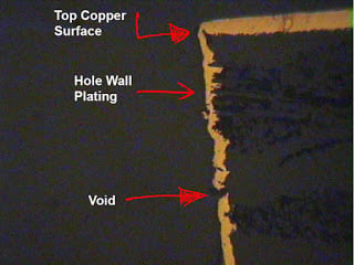
PCB with Copper Voids on the Inside of a Plated Through Hole
Problems with Deposition
Problems with deposition can compromise the interconnections inside the hole-walls, and will cause the PCB to fail. The most common deposition defect is the presence of plating voids in the copper lining the hole-wall. If the walls of the holes are not smoothly and completely coated, electrical current cannot pass through. The image above demonstrates a cross section of a through hole where the copper on the walls is much too thin, most likely as a result of poor deposition and plating.
Plating voids in plated through holes happen when, during the deposition process, copper is not coated evenly, preventing proper plating. This could be because of contamination, air bubbles in the sides of the hole, and/or rough drilling. All of these can create an uneven surface on the walls of the through hole, which make it difficult to apply a smooth, continuous line of copper.
Preventing Plating Voids In Circuit Boards
The best way to prevent PCB plating voids caused by rough drilling is simply to make sure to follow the manufacturer's directions during use. Manufacturers usually have a suggestion for the recommended number of drill hits and the correct in-feeds and speeds for the drill. A drill that is going down too fast can actually shatter material on its way down, creating a rough surface that is difficult to coat evenly during deposition and plating. If the drill speed is too slow, drill smear may occur, though it can be rectified during desmearing.
Key Takeaways
- Plated Through Holes Enable Multi-Layer Connectivity: They are essential in two-layer or multi-layer PCBs, providing conductive pathways between layers by electroplating copper onto drilled hole walls.
- Copper Deposition Is a Critical Step: A thin electroless copper layer is chemically bonded inside the holes before electroplating to ensure full conductivity and proper copper build-up.
- Plating Voids Are a Common Failure Point: Voids occur when copper fails to coat the hole walls evenly, often caused by contamination, trapped air bubbles, or rough drilling, compromising electrical interconnections.
- Drilling Quality Directly Affects Plating: Incorrect drilling feeds and speeds can create rough hole walls or smear, making it difficult to achieve a smooth, continuous copper layer during plating.
- Prevention Requires Process Control: Following manufacturer guidelines for drill usage (bit condition, speeds, hit counts) and ensuring proper desmearing and cleaning are key to avoiding plating defects.


