Printed circuit boards (PCBs) continue to shrink. As each generation of miniaturized components comes along, board designers find themselves able to work within ever-smaller PCB footprint sizes. While this is great news for consumers (compare the size of a 1994 portable phone to one of today’s models) it presents difficulties for fabricators.
Investment in Equipment
With each increase in PCB layout density, it is necessary to invest in new equipment capable of meeting increasingly difficult requirements for drilling, imaging, etching, and legend printing. There is often a period between when the designs first become more dense and the fabricators (who do not have unlimited funds) are able to catch up with the new equipment and methods necessary to build the boards at acceptable cost and acceptable scrap rates.
Designers can improve their chances for success by paying attention to some of the challenges and by adjusting non-critical elements of their tightly-spaced designs. A larger processing window for manufacturing benefits everybody.
Understanding The PCB Design Requirements
It is first necessary to understand which design requirements will pose problems. For starters, familiarity with standard design rules is most useful. Beyond basic PCB design rules, it helps to understand how fabricators deal with processing at the limits.
One common issue is that holes are getting smaller and smaller, but the limitations of mechanical drilling remain about the same with most manufacturers not able to reliably drill and plate anything smaller than 2.0mm (0.0079”) through a 0.062”-thick PCB.
Laser microvias are an option (and sometimes an unavoidable necessity) but in addition to being a costly process in itself, laser drilling often brings with it the necessity for costly sequential lamination.
Laser vias also limit your options for dielectric thickness because it’s necessary to observe an aspect ratio of about 1.25:1 (separation thickness vs. hole diameter) beyond which the resulting hole will be impossible to plate.
It’s best therefore, to avoid laser drilling whenever practical.
Designing a Thinner Circuit Board
One way to do this is to make the PCB thinner. While 0.0079” is usually the smallest drill offered for 1.5mm/0.062” thick boards, some fabricators are able to drill 0.0059” vias through boards up to about 1.0mm/0.039” thick.
With the thinner section, there is less drill breakage than with a standard thickness board. More important is the reduction in aspect ratio, which makes it possible for plating solution to pass through the shallower holes unimpeded, resulting in more consistent plating coverage and more reliable holes.

Teardrop Smallest Via
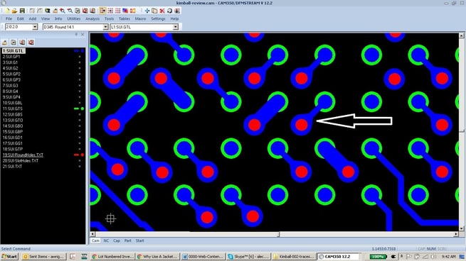
You can also minimize the pad size in relation to the via. Unlike component holes, vias only need pads that are 0.006” larger than the drilled hole. Although this seems to violate the IPC-2221 A+B+2C formula for meeting annular ring requirements, it is OK as long as you add teardrops to the pad-to-trace junctions (where annular ring is critical for reliability) and as long as you express the tolerance as 0.008” (or 0.006”) +0.000/-(hole diameter.)
This tolerance tells the fabricator that they can use the via diameter as the actual drill bit size (not the finished hole size plus an allowance for plating, as is normal for component holes) and that the final size of the hole is not critical, as long as there is at least the minimum acceptable amount of plating in the holes.
Most vias can’t be measured at final inspection anyway, since they will almost always be at least partially filled with soldermask, so as long as ampacity and connectivity requirements are met, finished hole size (FHS) is not important.
Copper-To-Copper Spacing
Local adjustment of copper-to-copper spacing values at the design stage can improve the process window so that it’s not tighter than it needs to be. The more spacing exists between copper features the easier it is for the fabricator to image and etch the circuitry accurately. It may seem counter intuitive to discover that one of the final steps in pre-production CAM artwork preparation is to increase the size of all the copper features, which effectively decreases the spacing. This may seem like an unauthorized design change, as well as a bad idea, but it’s actually neither.
Fabricators make these adjustments to the size of all copper features on a layer for a good reason. The actual amount of increase is based on statistical process data, which indicates how much of the copper feature size is expected to be lost while etching at an average conveyor line speed.
This number is generally in the neighborhood of 0.001” per ounce of surface copper. The reason this “etch adjustment” is not a true design change is that it’s temporary – the goal is to have all of the features etch back to their original, as-designed feature sizes.
There is a processing downside though. Film adhesion between the copper features begins to suffer as the spacing decreases, below a certain point the film can actually lift from the surface and fold over onto adjacent copper features, causing a short. Even if there are no film adhesion issues, etching the copper from between two copper features (particularly longish parallel runs) can be difficult and any incompletely-etched point will result in a short.
While in-process Automated Optical Inspection should identify and flag these defects, they cannot always be repaired, so your order may end up needing to be partially re-started in order to prevent a short shipment. To reduce the likelihood of such a negative outcome, it’s helpful to adjust your design to use more than the minimum copper-to-copper spacing value wherever the minimum is not absolutely necessary.

Pour Too Close
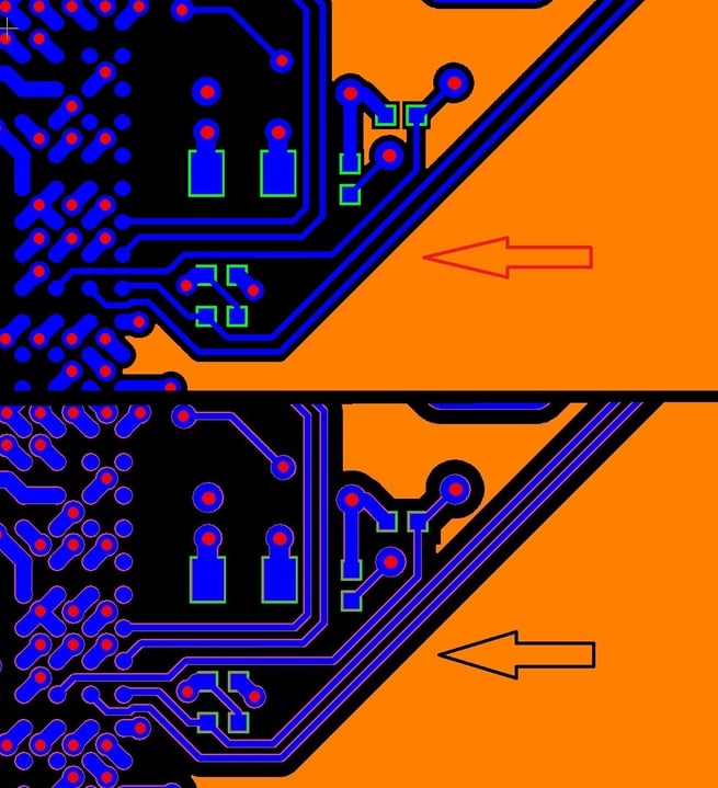
One opportunity for improvement is to use a larger keep-out value between copper pours and adjacent traces or pads. Most CAD layout programs will permit you to select a pour keep-out value that is different from the basic circuit routing design rules; we suggest that it’s well worth using this feature.
For example, on a design that uses .004” trace/space design rules, increase the distance from any surrounding pour to a larger value – at least 2x the design spacing if possible. Not only will this reduce the potential for unnecessary shorts caused by under-etching between traces and planes, but it will also eliminate coplanar interactions that could affect the performance of controlled impedance traces.
Summary
These are just a few suggestions that will help to improve yields on PCBs with tight spacing. For a more in-depth look, our Ebook, Top 10 Circuit Board Design Checks includes some additional tips having to do with Gerber output resolution, BGA soldermask setup, and internal via direct-connections, which are specific to tightly-spaced board designs.
It also includes more general tips about PCB design considerations and improvements that are easily overlooked, but which, when implemented, can help your prototype orders run cleanly, and your production orders run more repeatedly.
Key Takeaways
- Equipment investment is unavoidable: As PCB layouts grow denser, fabricators must upgrade drilling, imaging, etching, and printing equipment to meet tighter tolerances without driving up scrap rates.
- Laser microvias add cost and constraints: While they allow smaller holes, they require sequential lamination and have strict aspect ratio limits, making them best avoided unless absolutely necessary.
- Thinner boards enable smaller vias: Reducing board thickness lowers aspect ratios, improves plating reliability, and allows for smaller drill sizes without excessive drill breakage.
- Copper-to-copper spacing impacts manufacturability: More generous spacing reduces etching defects and shorts; designers should exceed minimum spacing rules, when possible, especially near copper pours.
- Design adjustments improve yield: Techniques like using teardrops at via connections, adjusting pour keep-outs, and tailoring tolerances help fabricators achieve higher reliability and repeatability in production.


