When designing and manufacturing passive broadband high frequency cascaded LC filters (inductor and capacitor), a lot of undesirable component interactions can occur if not properly managed. The goal is to minimize the difference between an RF microwave filter design constructed with ideal components and one using commercial off-the-shelf (COTS) and custom manufactured components.
Limitations of these components are frequency dependent but various techniques can be employed to improve their performance and reduce their impact on the microwave filter's overall electrical response.
The two essential components found on every LC filter circuitry are inductors (L) and capacitors (C). Unwanted distributed electromagnetic coupling can occur between these components but various techniques can be used to reduce these unwanted effects and minimize the deviation from a filter's ideal performance. Above all else, the choices made impact frequency of operation, power handling capability, and temperature stability.
Microwave Filter Components
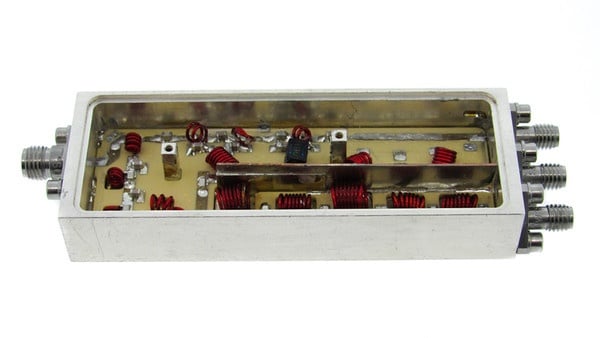
The lumped element component values realized using software analysis is considered to be ideal. In reality, these components occupy three-dimensional space. A consequence of components co-located in this space is reactive coupling with other components. The key problem for capacitors is the distributed inductance of the components exposed contacts.
 RF Filter Depicting Lumped Element Components
Inductors contend with distributed capacitance between turns tend to be sensitive to their installed environment because of their physical size. These characteristics can cause magnetic and electric coupling to their surrounding components. Additionally, unwanted losses can be influenced by the volume of solder used to connect the components to the circuitry.
Capacitor Effects
Placing capacitors in parallel is utilized when the component values called for in the design are non-standard values. It is also possible to connect capacitors in series in order to obtain non-standard values. Both techniques allow for a custom tailoring of the circuit but in either case, the distributed inductance can impact the actual capacitance value.

Example of RF Filter with Capacitors in Parallel
The effects can be minimized by using similar capacitor values with similar self-resonant characteristics. The larger the difference between the two, the more effect it can have on loss and attenuation. Manufacturers supply components with the capacitance measured and marked on the case. This capacitance can be modified by the component's distributed inductance and most of this inductance is contained in the lead length of the circuit. These should be kept as short as possible to avoid an increase in the distributed inductance.
Inductor Effects
Unlike capacitors, which are off the shelf components, inductors are usually custom fabricated to print. Factors that influence the specification are size constraints dictated by the filter order and physical space available the filter can occupy, required inductance, power handling requirements, desired Quality Factor, and frequency of operation.
Inductors also differ from capacitors in that they are more affected by the location where they are installed. Their physical size increases the electric and magnetic coupling to the surrounding components. The distributed capacitance of an inductor, between the turns of the inductor and to the surrounding components, can change the inductance. A coil's distributed capacitance can be reduced by winding the coils with finer wire and slightly increasing the spacing between the turns. Properly designed air wound coils used in series with capacitors provide stable inductance over temperature and frequency. Choosing your wire diameter, insulation type, and mounting orientation are the three main criteria.
Solder Effects
Copper is a very good conductor but printed circuit boards (PCBs) introduce signal losses that increase at higher frequencies. The calculated losses on a Microstrip PCB design, beyond the loss of the circuit itself, are a combination of conductor and dielectric losses. The resulting insertion loss can be improved through the use of silver plating over the bare copper. This plating also provides a superior surface for soldering of the components. Unfortunately, tin/lead solder introduces loss back to the circuit and therefore control regarding the amount of solder is extremely important. The correct amount must be applied to meet the IPC-Class requirement but must not be allowed to flow to the associated transmission lines.
Minimizing Component Interference
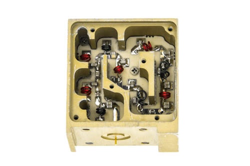
Component placement and RF shielding within the enclosure are critical to effectively reduce the inherent coupling between capacitors and inductors. Complete mechanical shielding is generally achieved by isolating the components to be shielded in a fully enclosed cavity.

RF Circuit with Mechanical Shielding
This is not always possible in a compact design; therefore, more than one method must be used. In conjunction with mechanical shielding, component placement can assist in reducing the effects of coupling. When inductors are co-located, the coils can be placed at right angles to each other. Another method is to keep the coils at least as far apart from one another as their outside diameter. Both methods must also be mindful of the lead placement as they relate to the capacitor location and possible distributed inductance.
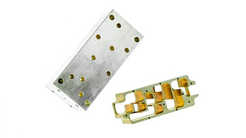
One method to offset this is to reduce the line width or length of the printed circuit board trace but must be carefully done to avoid affecting impedance. The capacitor orientation can also be maximized by mounting the component in a vertical orientation rather than the traditional horizontal position. Mechanical shielding can be achieved by creating a network of machined pockets for each capacitor/inductor network. This can complicate the design but can also yield dramatic results if the proper materials are used and contiguous grounding is maintained.
Summary
Microwave filter design success lies in the ability to find a balance of the MicrostripPCB layout, capacitor and inductor component placement, solder volume, and mechanical shielding.
Distributed inductance of the through path of a filter circuit causes a gradual increase of associated losses that can be minimized or eliminated with various design and construction techniques that isolate the component interference and parasitic resonances. The physical size of capacitors and air wound inductors makes them susceptible to internal and external capacitive coupling.
Key Takeaways
- Capacitors introduce distributed inductance through their leads, which can alter actual capacitance values; keeping leads short and using matched capacitor pairs helps minimize losses.
- Inductors are highly environment-sensitive, with distributed capacitance between turns and nearby components affecting inductance; coil spacing, wire size, and orientation are key design factors.
- Solder volume impacts RF performance, as excess solder can increase loss at higher frequencies, making precise solder control critical.
- Component placement and shielding reduce coupling, with strategies like orienting inductors at right angles, spacing coils apart, and isolating parts in shielded cavities.
- Filter performance depends on balancing multiple factors - PCB layout, component design, solder management, and shielding to minimize interference and maintain stable operation across frequencies.


