If you’re a designer of RF or microwave printed circuit boards you’ve probably already selected a laminate material that is appropriate to your project, having based your choice primarily on the electrical requirements of the circuit, such as signal speed, loss rate etc. Be careful, however, not to overlook the fact that the specialty materials used in such designs also possess unusual mechanical characteristics; processing is different from that of normal FR4 boards.
It is critical given the high cost and occasional procurement difficulties associated with such laminates that you select a fabricator who has experience dealing with their peculiarities. Such a fabricator will avoid creating expensive scrap by anticipating problems and by utilizing tools, processes, and chemistries that will guarantee a high yield.

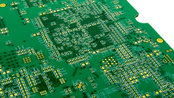
PCB Manufactured with RF Laminate Material
Below is a brief overview of some common difficulties inherent in high frequency PCB manufacturing.
Scaling
Most circuit board fabricators understand the concept of artwork scaling from years of building FR4 multilayer PCBs where internal layers lose some mass as they are cured during heat lamination. The circuitry is scaled-up by known percentages in anticipation of this loss so that the layers will return to their as-designed dimensions after the lamination cycle is complete.
High frequency laminate materials being softer than FR4, behave somewhat differently but the idea is similar to figure out and compensate ahead of time for what the material is likely to do as it moves through the process. This means that separate scale factors must be established for each type and even for each thickness within a type in order to guarantee repeatability. Otherwise, registration from drill to pad and from layer to layer may be compromised, adversely affecting the performance of the finished circuit board.
The fabricator will use the laminate manufacturer’s baseline scaling recommendations in combination with in-house statistical process control data, to dial-in scale factors that will be consistent over time within that particular manufacturing environment.
Surface Preparation
Multilayer surface preparation is critical in order to get a secure bond between layers. This is especially true with PTFE (Teflon) types. If the preparation is too aggressive, the relatively soft material can become deformed. If the deformation is significant, then registration will be poor and the entire PCB (or multiple PCBs on a panel) may end up as non-functional scrap.
Deburring if not done properly can actually polish the substrate. This will adversely affect adhesion in multilayers remember that some of these materials consist of nearly-pure Teflon, a product already famous for its “non-stick” nature.
Replacing these materials is costly and can result in long delays. This is another instance where an experienced fabricator will be aware ahead of time that the only way to avoid a bad outcome is to anticipate the need for special handling and to take the appropriate steps to be sure that the process is done carefully and correctly.
Hole Preparation
Before plating through with copper, all holes on an FR4 PCB must be treated to remove debris, surface irregularities, and epoxy smear so that the plating will adhere to the hole walls. RF materials, which typically include PTFE / Teflon or ceramic, require different methods of hole preparation.
Early in the process, drill machine parameters are adjusted to prevent the substrate from smearing in the first place. Then, when the holes are treated after drilling, the plasma cycle uses different gases from “normal” boards. Failure to adequately prepare the holes before plating will result in poor interconnections which may fail over time. It is therefore critical for long-term reliability to plan and follow the steps necessary to form clean holes that will accept plating.
Thermal Expansion Rates
The CTE (coefficient of thermal expansion) is critical to long-term reliability. It is a measure of the amount of expansion the material will undergo in any of the three axes (X, Y, or Z) under thermal stress. The lower the CTE, the less likely the plated through holes are to fail from repeated flexing of the copper which forms the internal layer interconnections.
CTE can become complicated in instances where high frequency materials are combined with FR4 in “hybrid” multilayer PCB constructions because the CTE of one material must match that of the other material closely or the different layers will expand at different rates.
The same is true of any hole fill material used for plugging vias. It needs to be matched to the other material(s) in the stack. A fabricator accustomed to dealing with the various materials will be able to analyze the combination to be sure that it is appropriate.
Machining
There are some RF materials that are formulated so that they will behave very similarly to the more familiar FR4 laminates when they are machined but it is useful to understand some of the differences. For example, drilling through ceramic-impregnated types can be very hard on drill bits so it is necessary to reduce maximum hit counts and to customize spindle infeed and RPM settings. Fibers may remain inside hole walls. These are difficult to remove prior to plating so again, the adjustments to the drilling parameters are intended to minimize their occurrence.
Routing is best performed using special bits developed specifically for RF laminates; otherwise the edge quality will be poor. An RF circuit board routed with the incorrect router type will be instantly recognizable for its furry edge quality which indicates pulling of the tool against the random fibers. Similarly, a v-scoring machine’s saw blade can tear some materials and will often pull the copper up from the surface. Perforated edges may be more flexible than with FR4 and may not allow for clean breaking. With a few exceptions (such as boards which combine RF layers with FR4 layers) v-scoring is generally not a recommended process for these materials.
It is very important to understand the differences between machining RF laminates and machining FR4 so there are no unwelcome surprises. Successful job setup means buying the correct tools and making the appropriate processing adjustments before something goes wrong, not after.
Summary
Building high-frequency PCBs is certainly not impossible. With the right type and amount of planning they are only marginally more difficult to manufacture than standard FR4-types. They do however require a fair degree of experience in production planning, as well as some tools and processes specifically optimized for this sort of work. When the time comes to build your PCB, be sure that the fabricator you choose has the right equipment and experience to produce it correctly on the first try.
Key Takeaways
- Scaling requires precision: RF laminates expand and contract differently than FR4, so fabricators must establish unique scale factors for each material and thickness to maintain registration and performance.
- Surface preparation is delicate: Soft PTFE and other RF materials can deform under aggressive prep, and improper deburring may harm adhesion, making specialized handling essential.
- Hole preparation is different from FR4: Drilling parameters and plasma treatments must be adjusted for PTFE or ceramic-based laminates to avoid smear and ensure reliable copper plating in vias.
- Thermal expansion mismatches can cause failure: In hybrid designs that combine RF laminates with FR4, mismatched CTE values between layers or fill materials can stress vias and interconnects.
- Machining needs special tools and methods: Routing, drilling, and scoring RF materials demand dedicated bits and processes; otherwise, edge quality, copper integrity, and yield are compromised.


