Two existing filter designs will be used as examples – A 3-port LC diplexer, with passbands from 100-500MHz and 700MHz-6GHz, and a suspended substrate distributed element broadband bandpass filter, with passband from 2.5-6GHz.
Capacitor Tolerance
The capacitors used in the LC diplexer design are +/-5% tolerance over nominal. Each capacitor forms a pole in the pass band, so the variance in frequency of each of the poles will affect the electrical response of the filter. The response of the diplexer with nominal capacitance values is shown in Figure 1. A yield analysis of varying capacitor values over the +/- 5% tolerance is shown in Figure 2. It shows a yield of 65%, meaning 35% of manufactured parts would need to be tuned to meet the electrical spec.
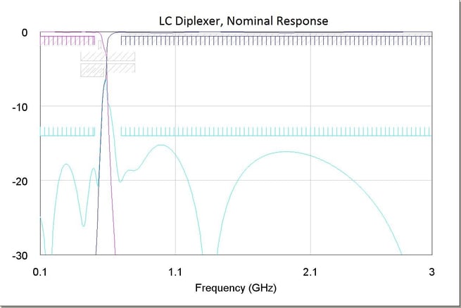
Figure 1: LC Diplexer, Nominal Response
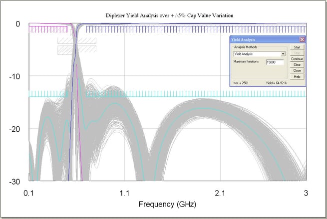
Figure 2: Diplexer Yield Analysis
Since chip capacitors are used in this design, tuning a capacitor directly can be a challenge. In some cases, they can be detuned with tuning screws, but the technician is usually limited to desoldering the part and installing a different value capacitor, or installing 2 capacitors in series or parallel to get a between value. This process can be arduous and permutations are limited to the time taken to change components. Alternatively, since air-coil inductors are used in the design, the off-value capacitances can be offset by tuning the inductor values, which is a much faster process. Inductors can be lowered by spreading coils farther apart, or raised by compressing coils together. This process can be performed in real time on the test bench by the test technician, while observing the response on the network analyzer. The technician can jump between different inductors quickly, making the tuning process much more efficient than trying to tune the capacitors.
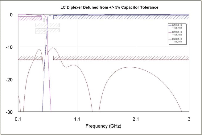
Figure 3: LC Diplexer Detuned from +/- 5% Capacitor Tolerance
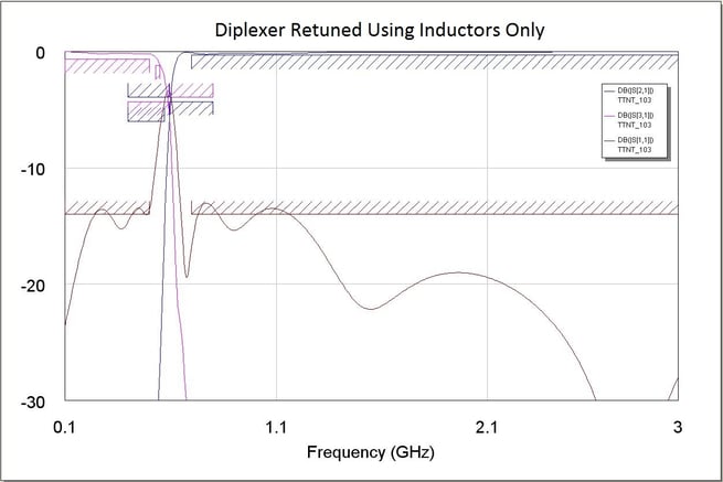
Figure 4: Diplexer Retuned Using Inductors Only
Figure 3 shows one of the worst case responses from Figure 2, due to capacitance tolerance. Figure 4 shows a retuned diplexer with constant capacitance values from the Figure 3 circuit, and retuning using inductors only, simulating a practical bench tune. The result is slightly out of spec on return loss, but much closer than in Figure 3, resulting in minimum capacitance tuning needed to bring the filter into specification.
Material Properties
The RF dielectric material used on the suspended bandpass is .005” thick, with a +/- .0005” tolerance. It has a dielectric constant of 2.20, with a manufacturing tolerance of +/- .02. Each of these tolerances can impact filter response; material may need to be screened for thickness variation or smaller panel sizes chosen. Figure 5 shows the suspended filter nominal response. Figure 6 is a yield analysis of the filter over dielectric thickness variance. Figure 7 shows the filter over a 5% Dk variance.
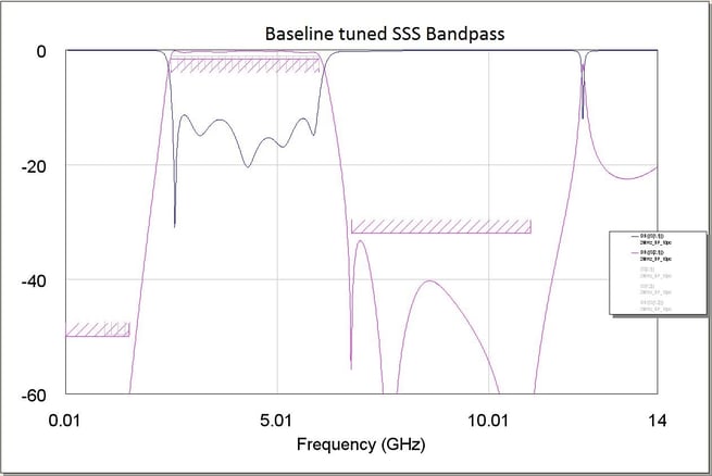
Figure 5: Baseline Tuned SSS Bandpass
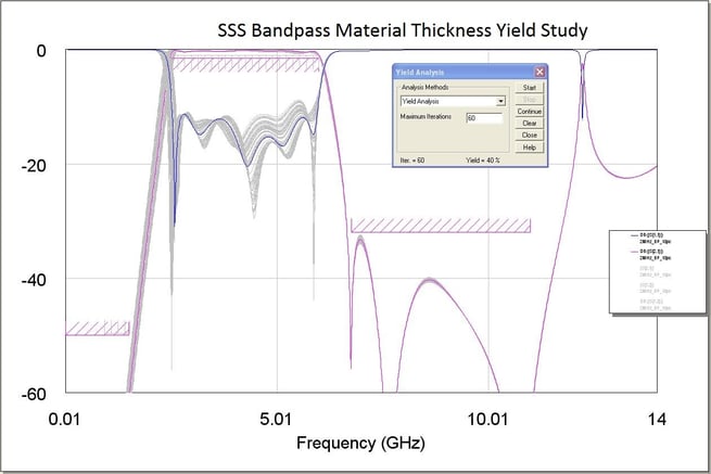
Figure 6: SSS Bandpass Material Thickness Yield Study
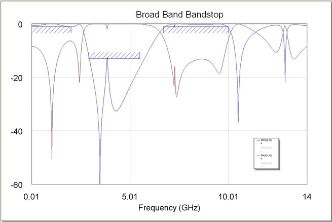
Figure 7: Broad Band Bandpass
In this case, material thickness variation has a large impact on the filter performance. This impact is realized mostly in the capacitive couplers that are part of the high pass filter portion of the response. The capacitor values are directly proportional to the thickness of the substrate between plates. The dielectric thickness variance creates a 40% yield for this product, and it must have active tuning in order to increase yields. Tuning on suspended substrate product can be performed using capacitive tuning screws or slugs to adjust capacitance to ground at any point in the circuit, or cutting and adding metal to traces directly on the PCB to change impedances.
This filter does not vary much over a 5% Dk tolerance sweep, which in itself is more than expected in the real-world application. It is designed with some margin at the spec edges for insertion loss and isolation, allowing the slight frequency shift seen in Figure 5.
Etch Tolerance
At PCB fabrication, the transmission lines are etched from the copper that is laminated to the dielectric substrate. The transmission line widths formed during etch typically carry a tolerance of +/- 0.001” per ounce of copper (copper is 0.0013” thick per ounce). Figure 8 shows the SSS bandpass filter response as varied over the etch tolerance. There is not a large deviation in this case for broadwall coupled capacitors. Etch tolerance would have a large response for edge-coupled capacitors as in an edge-coupled microstrip design.
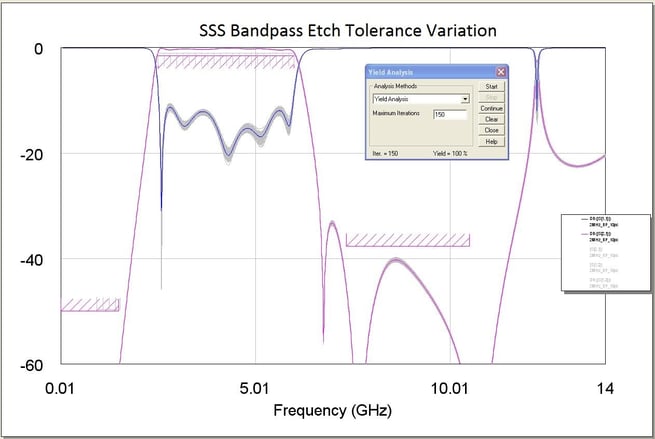
Figure 8: SSS Bandpass Etch Tolerance
Further Manufacturing Tolerance Impacts
The height of the cover, or ground reference can affect the impedance of the lines that reference it, especially in the case of the SSS filters. The launch from connector to PCB will affect the electrical response of the filters as well. Tight radius as small as .016” as well as shallow pockets measuring as little as .022” require tight controls. All dimensions and tolerances apply after plating so cumulative stack up tolerances are critical as well.
The launch from connector to PCB will affect the electrical response of the filters as well. This study is not within the breadth of this article, as it would require running simulations in a full 3D modeler.
Summary
To ensure the greatest possible functionality of the end product, it is imperative to simulate full manufacturing tolerance sweeps for critical specs in RF filter design. Many passive components can be designed with extra margin on the specs. A bandpass filter can be designed with margin on bandwidth, but will need extra poles to meet the isolation spec. The extra poles add loss (and package size) so pole # selection should be done with care – the minimum number needed to reach response spec with acceptable amount of tuning predicted.
Key Takeaways
- Capacitor tolerances have a major impact on filter yield: In the LC diplexer example, +/-5% capacitor variation resulted in only about 65% of units meeting spec without tuning, showing how critical capacitor accuracy is.
- Inductor tuning is often more practical than capacitor tuning: While capacitors are difficult to adjust, inductors can be fine-tuned in real time by compressing or spreading coils, making them an efficient way to offset capacitance variation.
- Dielectric thickness variation significantly affects suspended substrate filters: A tolerance of +/-0.0005” caused a 40% yield in one design, making active tuning methods like tuning screws or trace modification necessary.
- Etch tolerance effects depend on capacitor type: For broadwall coupled capacitors, etch tolerance had minimal impact, but edge-coupled designs are far more sensitive to width variations from PCB fabrication.
- Stack-up and mechanical tolerances also influence performance: Cover height, plating thickness, connector transitions, and cumulative tolerances all contribute to impedance shifts and electrical deviations, highlighting the importance of simulating full tolerance sweeps in design.


