


Nobody wants to experience the feeling of populating your new printed circuit board (PCB) design and finding out that it is not electrically functional. Most often, the lack of functionality is attributable to a specific production problem or a combination of several different problems. Sometimes, however, the problem is that the Gerber files exported from your PCB CAD program contained an error that went unnoticed because there was no way to verify that the files matched your design intent. You can avoid a good deal of trouble by supplying an IPC-356 format netlist file with your fabrication data package.
Below is a brief overview of some of the things that can go wrong and how a netlist file helps to catch potential problems at the pre-production stage, instead of on your test bench.

How the Netlist Is Used Before Editing
The netlist file (formatted as IPC-356) is nothing more than an ASCII text file that includes instructions for the PCB CAM software such as net names, pin, and XY locations of start and end points for each net or node. If the customer supplies an IPC-356 netlist then it is read in during the initial Gerber file load.
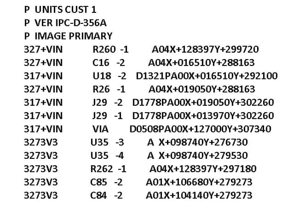
Example of a PCB Netlist File as Viewed in any Standard Text Editor
After loading and placing the Gerber layers into a logical sequence from top to bottom, we use our CAM program to assign a type to each layer. Once the layers are defined electrically, we generate a reference netlist, based on Gerber and drill data. The CAM program identifies areas of COLOR as copper, areas of BLACK as absence of copper, and follows the layer to layer interconnections through the plated through holes.
The CAM program then compares your IPC-356 netlist to the Gerber-derived reference netlist. We report any discrepancies to you and resolve them before moving forward. We do request that the designer call out any known anomalies that we may discover (such as intentional shorts) ahead of time on their drawing or in a separate information file. If they are not called out in the other supporting documentation as requested, then we are obliged to stop and resolve such discrepancies before we can proceed.
Possible Causes of Discrepancies
One might think that Gerber files are infallible and since the industry universally adopted RS274X and ODB++ as standard import formats, they are, in fact, nearly so. However, it is still possible for errors to occur.
Features that are incorrectly described in the Gerber file header during importation will change the system’s interpretation of the desired electrical path leading to incorrect nets being defined in the Gerber-derived reference netlist. Corrupted features may include incorrect-sized pads or unfilled polygons. For example, occasionally a self-intersecting polygon will resolve incorrectly (usually because the Gerber file resolution is not fine enough). This can cause the polygon fill to leak through what the CAM program interprets as a keep-out that is not fully closed. What is intended to be a clearance then floods with copper, shorting the hole and the surrounding plane. Exporting your Gerber files with the highest possible resolution (2:6 if possible) or choosing line fill instead of polygons will help you to avoid this issue but supplying a netlist is still recommended.
Operator setup errors can also cause the CAM program to misunderstand what it is looking at. The most common problem is a simple operator error when assigning the layer types immediately after importing the raw files. If a negative plane is assigned as positive, or vice-versa, the CAM system will see the reverse of what it is supposed to see. The resulting netlist will be incorrect.
To explain: a layer with positive polarity appears in CAM as color = copper, black = absence of copper. A layer with negative polarity will be displayed the opposite way, with color = absence of copper, black = copper. When deriving the reference netlist, the CAM program interprets areas where copper is present as part of the board’s conductive path. If copper and absence of copper are reversed (because the operator has set the layer polarity incorrectly) then the CAM program will create a netlist that does not reflect the true design intent.
It is therefore best to supply internal layers with positive polarity whenever possible to minimize the chance for operator error. Regardless, the best fail-safe is to also supply a netlist file with the rest of your PCB Gerber files. If the operator runs the design netlist against the incorrect CAM reference netlist, and notices massive shorting or multiple opens, it is a simple matter to review the layer type and polarity assignments. After changing a few toggle settings, the operator can generate a new reference netlist and be back in business. Absent a customer-supplied netlist file, which can be compared to the Gerber-derived netlist, this error may go unnoticed until you perform an in-circuit test on a populated PCBA. By then, it is too late.
During CAM Editing
The netlist is kept active throughout the CAM session. When the CAM session is complete, we re-check to the netlist to be sure that no electrical shorts or opens have been created during editing. Then we make files for one of two test fixturing methods.
Electrical Test Fixturing
A hard test fixture is a plate of polycarbonate or a similar material. The plate is drilled with holes, which accept conductive probes. The probe locations match the end points of each circuit to be tested. Via (non-component) holes are generally omitted, either because they are mid-points on the net, or because they are covered by non-conductive mask and will show as false opens if probed.
Other mid-points are usually omitted as well, because the test machine has a finite number of grid positions available. Making sure that a probe is assigned to every end point takes priority over the testing of every single node. With or without mid-points, the continuity test is still 100% valid. It will pick up all short or open circuits so long as all endpoints are probed.
If a single plate cannot contact every net (as when a PCB uses SMT components on top and bottom) then it is necessary to use two plates. This method is known as clamshell testing. The clamshell uses two parallel fixture plates – one mounted facing up, the other facing down. Each plate is loaded with stationary probes that match the locations of each net’s end points. The two plates are then compressed to contact the top and bottom of the PCB simultaneously, in much the same way as a clam might close its shell. If the signals generated by the probes match the netlist, then the board passes the test.
Using the flying probe method, there is no fixture as such. Instead, the board is mounted between two fast-moving test probes. These are wired to the tester’s controller, which stores the netlist file. One probe contacts the end point pad of a net on the top layer, while the other contacts the end point pad on the bottom layer. If the circuit path between the two probes matches the path defined by the netlist, that net is judged to be good. The probes then move to the next set of end points, and so on, until the entire PCB has been tested.
If an IPC netlist is not supplied, then we use CAM software to extract a reference netlist from the Gerber and drill data, as described at the beginning. There is no choice but to assume that the Gerber files accurately reflect the electrical requirements for the board, and that they can be used for CAM editing checks and electrical test fixturing.
This is not as reliable as netlist testing. It resembles the old, pre-CAD method of “golden board” testing, where one board would be placed onto the tester and cycled, so the machine could “learn” the circuit. Absent a netlist, that board was necessarily assumed to be correct, and all subsequent boards were tested against it. The flaw in golden testing is that if all the boards in the lot, including the golden board, have the same defect built-in, then all will pass the continuity test, but they will all be wrong.
The same issue exists when using only a Gerber-derived netlist. While it is a perfectly acceptable method so long as the Gerber files do not contain errors, and the CAM operator assigns the correct layer types with the correct polarity, it is still possible for something to go wrong. A customer-supplied netlist exported directly from the CAD layout software provides an extra layer of verification that the board has been built correctly.

Summary
To add an extra degree of certainty that your PCB will function correctly, Epec suggests that if your PCB layout software supports the IPC-356 format, you should always take the time to export the file and send it to your fabricator.
Key Takeaways:
- Definition and Importance of a PCB Netlist: A PCB netlist is an IPC-356 format ASCII file that defines electrical connections, including net names, pin locations, and XY coordinates, ensuring design intent matches the final PCB.
- Purpose in PCB Fabrication: Netlists help verify that Gerber files are free from errors and reflect the intended electrical paths, avoiding costly production issues.
- Error Prevention: The netlist catches discrepancies like incorrect layer polarity assignments, corrupted features (e.g., self-intersecting polygons), or operator setup errors during CAM processing.
- Comparison and Verification: During the CAM process, the IPC-356 netlist is compared to a Gerber-derived reference netlist to identify discrepancies, such as unintentional shorts or opens.
- Applications in Testing: Netlists are used to create hard test fixtures or flying probe setups, ensuring accurate continuity and identifying electrical issues before assembly.
- Discrepancies Without a Netlist: In the absence of a netlist, errors in Gerber files or operator setup might go unnoticed until functional testing, increasing the risk of failed boards.
- Best Practices: Always supply a netlist with your Gerber files and other fabrication data to ensure robust error detection and streamlined manufacturing.
- Golden Netlist Drawback: Relying on a system-generated or "golden" netlist can propagate errors across all boards if the initial netlist has inaccuracies.
- Recommendations:
- Use IPC-356 format for compatibility.
- Export Gerber files at high resolution (e.g., 2:6) to minimize interpretation errors.
- Document intentional design anomalies clearly to avoid unnecessary stops during the fabrication process.


