


Designing a PCB with extreme copper plating requires planning and careful consideration of several factors that do not come up during the design of a standard, light copper board. Many fabricators avoid heavy and extreme copper circuit board orders entirely because of the unusual manufacturing challenges and non-standard processes associated with these product types.
Even under the best circumstances, extreme copper circuit boards are likely to remain significantly more difficult than normal to build. It is, however, still possible to create a manufacturable design by learning about the difficulties inherent in extreme copper PCB manufacturing.
This blog post will explain some important principles of the extreme copper plating process, thereby enabling PCB designers to make sound choices that will result in successful manufacturing.

Normal PCB Verses Extreme Copper PCB
The most obvious difference between a normal PCB and one that employs extreme copper is the amount of plating the circuit board receives. The difficulties inherent in applying such large amounts of copper plating (20 oz. and up) are the reason that only a handful of specialist PCB manufacturers will take on this style of work.
It is nevertheless possible, with good planning and some degree of experimentation, to eliminate or reduce the problems associated with such high plating. Still, it may be necessary to accept that some negatives are impossible to eliminate completely and to decide whether or not you can live with them in order to take advantage of the benefits of extreme copper.
Rules of Thumb for Trace Width and Spacing
Your printed circuit board fabricator will advise you about appropriate trace widths and spacing. Expect these to be larger than what you’re used to on lighter boards. There may also be two or more sets of rules. This is because the final determining factor in establishing rules is the weight of the base copper, not the finished copper. Although heavier base foil (up to 4 or 6 ounces) may shorten the plating time, that is probably the only advantage.
One disadvantage is that you will get a trapezoidal trace cross section caused by etching down through the heavy base foil. A trapezoidal trace has less current carrying capacity because the top of the trace is narrower than the base. The fabricator may also have problems drilling the plated holes through so much copper, as vacuum material removal during the stroke becomes more difficult when more copper is present. For these reasons, expect the fabricator to recommend starting with very light foil, such as half-ounce.
While using half-ounce foil to achieve a 20-oz, plate-up is counter-intuitive, it is superior in all ways to using heavier foil. With light foil, it becomes possible to use narrower traces and smaller spaces, so the area available for circuit routing on each layer increases.
Another advantage is that trace etching quality improves. Most importantly, because the entire trace sidewall is formed by plating buildup, the sidewalls are almost perfectly perpendicular to the substrate after etching. The benefit here is that the cross-sectional area of the trace is exactly its height times its width. Because of this, you can design the traces with a lesser overall trace height after plating than would be possible by doing less plating on a thicker base foil and still meet the same current carrying capacity.
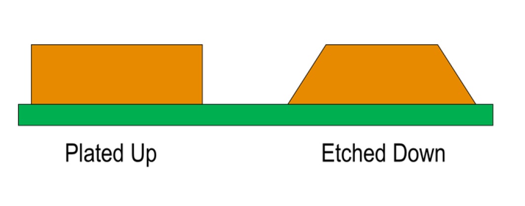
Note full cross section of the trace which is plated-up instead of etched.
Extreme Copper and Plated Through Holes
As in standard PCB manufacturing, the plating through of the holes and the plating up of the circuitry are part of a single process. For normal PCBs, the amount of added copper is small and predictable. The drill tools used to form the plated through holes (PTH) are typically sized about 0.003”-0.006” larger than the desired finished hole size (FHS). The amount of over-sizing depends upon the fabricator’s process controls as well as what final surface will be applied. Between the plated copper and the surface finish, the drilled hole will close down during processing to its nominal final diameter. Heavy and extreme copper is different.
For circuit boards plated with heavy and extreme copper, the holes can usually not be drilled to the significantly larger diameters that would be necessary to enable the holes to finish close to their nominal diameters. Consider, for example, a 20-oz. PCB. The surface is receiving about 0.028” of added copper. The holes are receiving a similar amount. Instead of adding 0.005” to the drill size before plating, as on a light copper board, it would be necessary to add almost 0.060” to such a hole. It is not difficult to imagine the adverse effect of adding 0.060” to the annular ring of every hole in the design; it would severely reduce the amount of surface area available for circuit routing. Beyond that obvious problem, the exact amount of plating each PTH receives becomes somewhat more random. Hitting a +/-0.003” tolerance in every location on the board becomes highly unlikely. What is the solution?
The solution is to perform a re-drill after plating, but before surface finish application. The re-drill removes the extra copper buildup, thereby restoring the hole to its correct nominal diameter. This works quite well and sounds like a perfectly elegant solution, but as with everything else related to extreme copper, there are pitfalls and limitations.
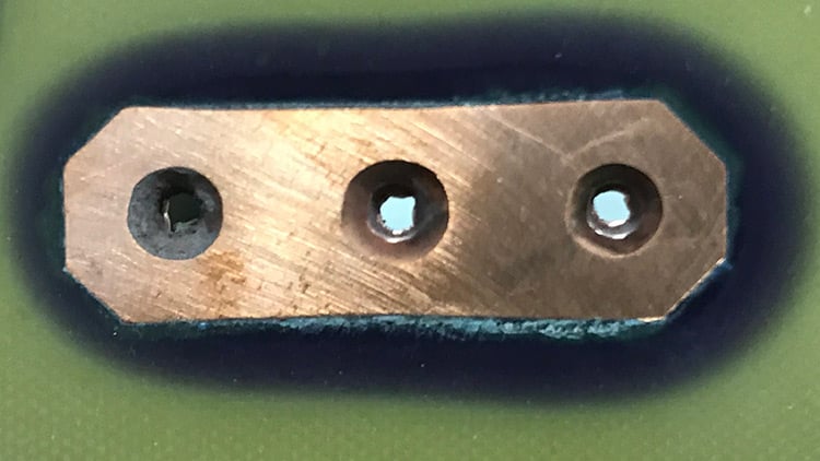
These holes will be machined later to remove the excess copper.
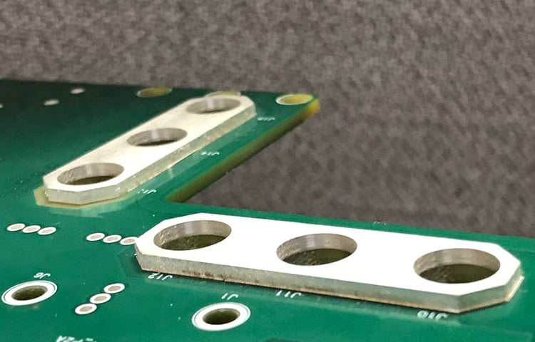
Here, the holes are at final diameter and silver coated.
The main problem is that the center of the hole does not close down into a perfectly flat surface that readily accepts a spinning drill bit. Instead, the plating tends to be somewhat rounded and concave, with a relatively small open area in its center. Drill bits want to deflect when they encounter a surface that is less than flat, and when carbide drills deflect, they snap. To overcome this problem, plan to use finished hole diameters starting at around 0.050.” Drills in this range are generally robust enough to survive their encounter with the concave surface, so long as the in-feed and RPM settings are adjusted for this non-standard application.
For holes that are not intended to accept components or wires, you may use smaller holes and allow the fabricator to simply plate them shut (or nearly shut). Even if the holes are nothing more than vias, it is still a good idea to make them larger than normal vias. This is particularly true for multilayers, which may have heavier than normal copper weights internally. Regardless of the number of layers, a good rule of thumb for extreme copper boards is to use vias which are drilled no smaller than 0.025” before plating, and preferably 0.030” or larger.

Summary
Extreme copper PCBs are never completely routine to design or to build. This is because each unusual feature may affect some other feature; the solution to one design requirement may present an insurmountable difficulty in another area. Plan ahead. Allow extra time for both the design and production cycles. Above all, ask questions. Your PCB fabricator can steer you away from potential dead ends early in the cycle. Submit a preliminary version of your layout for a design for manufacturing (DFM) review, to identify areas needing improvement.
The result of a partnership between PCB designer and manufacturer should be an extreme copper circuit board that will function with high reliably.
Key Takeaways
- Extreme Copper PCBs Require Specialized Design and Manufacturing: Designing PCBs with 20 oz. copper or more introduces significant challenges that most standard fabricators avoid. Success depends on understanding unique processes, careful planning, and partnering with experienced manufacturers.
- Use Lighter Base Copper for Better Trace Definition: Starting with a lighter base copper (like 0.5 oz) and plating up is preferable to using heavy base foil. This approach allows for narrower traces, better etching quality, and nearly vertical sidewalls, improving current capacity and layout flexibility.
- Re-Drilling Is Essential for Accurate Hole Sizes: Heavy copper plating drastically reduces hole diameters. To achieve precise finished hole sizes, a re-drill after plating is necessary. However, this process demands larger minimum hole sizes (typically 0.050") to avoid drill breakage.
- Design Vias Larger Than Standard: For extreme copper PCBs, standard via sizes isn’t sufficient. Designers should plan for vias drilled at least 0.025"–0.030" before plating to ensure reliability, especially in multilayer boards with heavy internal copper.
- Early DFM Reviews Help Avoid Critical Pitfalls: Extreme copper designs often involve trade-offs were solving one issue may create another. Engaging your PCB fabricator early for a Design for Manufacturing (DFM) review is crucial to identify risks, optimize the design, and ensure a manufacturable, high-reliability product.


