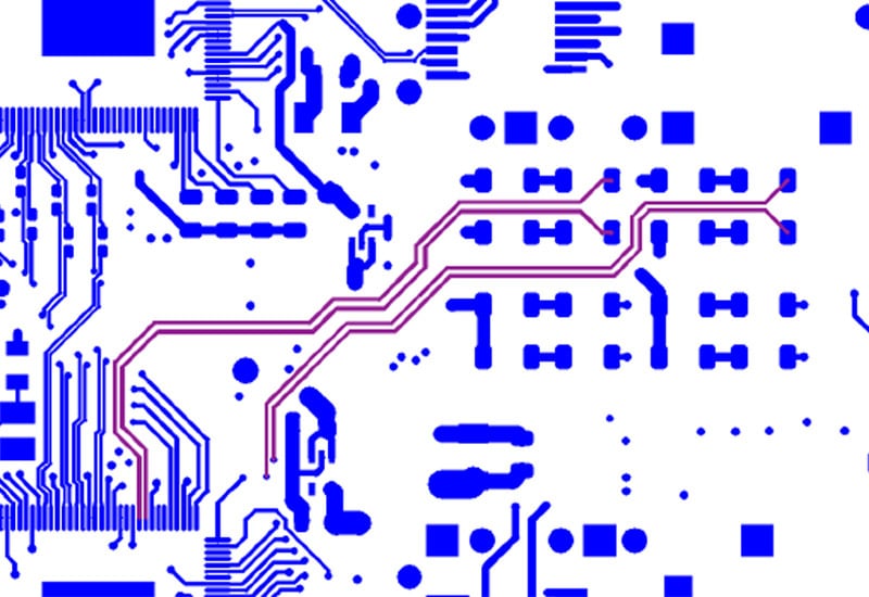
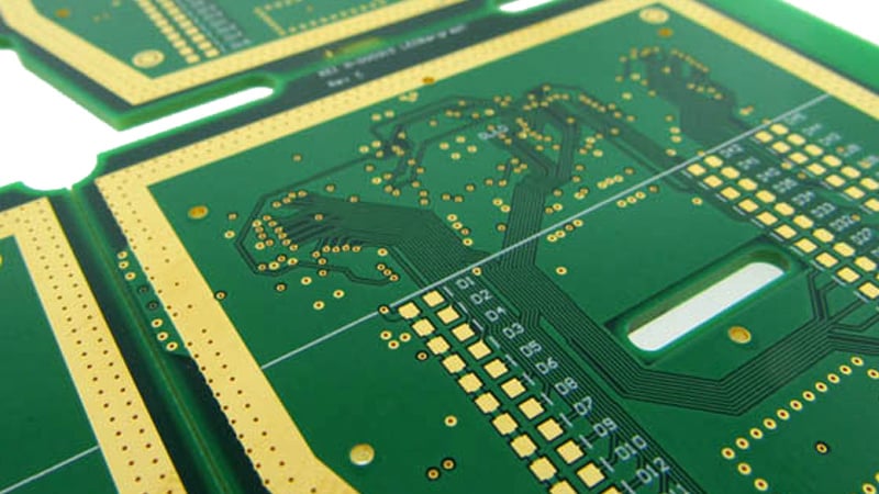
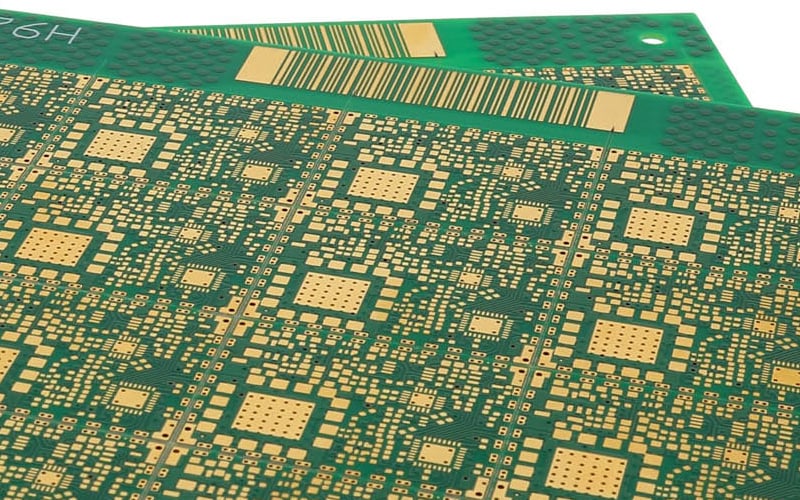
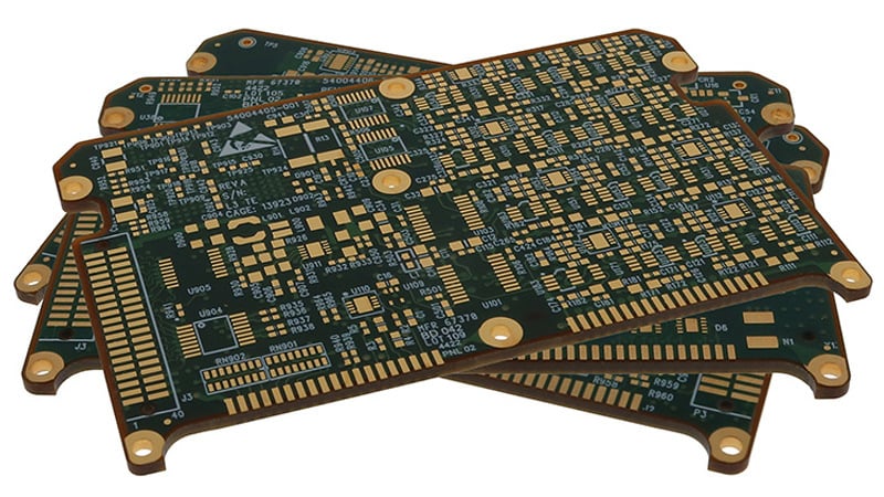
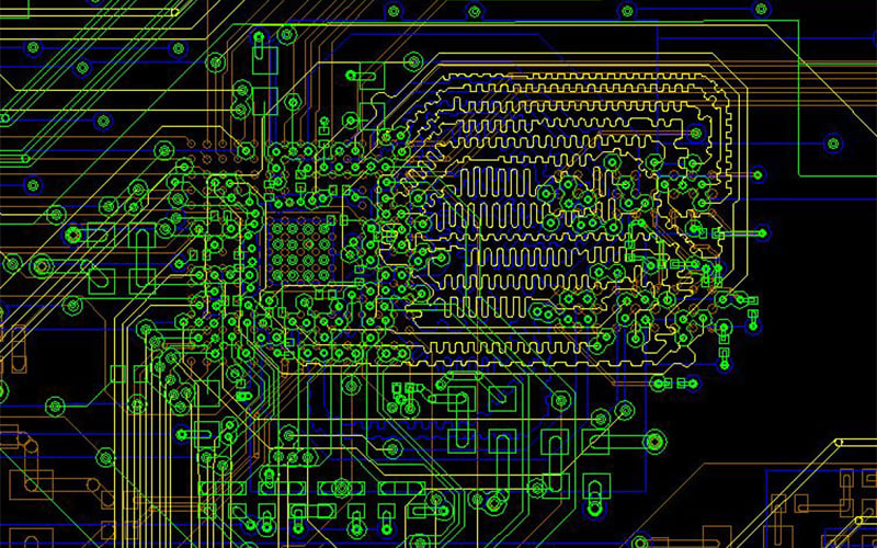
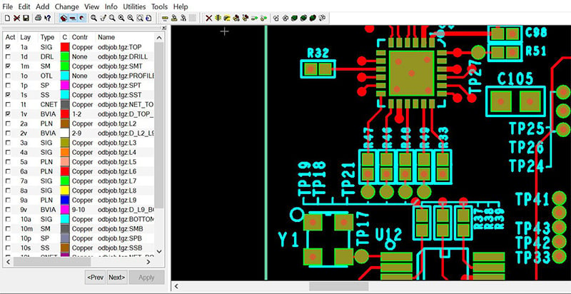
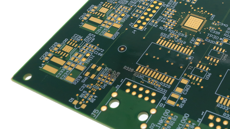
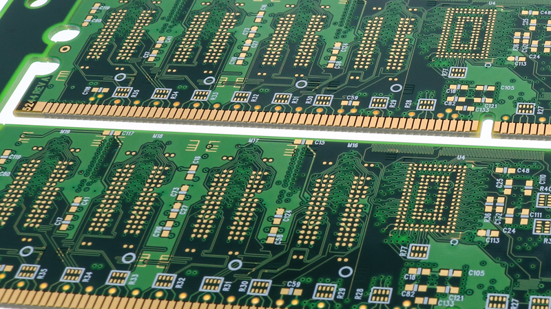
In today’s digital and electronic world, with higher frequency electronics and the miniaturization of devices, it is becoming increasingly important to effectively control the electrical signals in the high-speed printed circuit boards used.
Read MoreAngie Brown

Recent Posts
I sat at my desk contemplating the subject of this blog post, trace and space circuitry for printed circuit boards, and as usual, I drifted back to the start, for me, which was 1982. The date stamp amuses me – how is it 2024, already!? Of course, when you look back, you can’t stop the memories from flooding in.
Read MoreIn this post we will review these 2 types of markings and additional identification marks that can be incorporated into your printed circuit board.
Read MorePrinted circuit boards (PCBs) require insulation as part of the manufacturing process. The insulation helps to protect non-conductive materials while also preventing the conductive components from coming into contact with each other. It separates the conductive paths to prevent shortages and failures.
Read MorePrinted Circuit Boards (PCBs) are ubiquitous in today's technology-driven world, serving as the backbone for everything from smartphones to space shuttles. While they may seem straightforward, the truth is, no two PCBs are the same. With the advent of increasingly complex electronics, manufacturing PCBs has become an intricate task that involves a lot of specialized engineering.
Read MoreAt the base of all printed circuit boards is the material. We have to start somewhere, so, let’s talk about the material. PCBs are built-to-print products, and although they are very similar, no matter the shape, size, or layer count, they are unique and have their attributes.
Read MoreFrom powering everyday gadgets like smartphones and laptops to complex systems in medical devices and aerospace technology, printed circuit boards (PCBs) are fundamental to modern electronics. They are essentially the heart and soul of all the electronic gadgets and devices that we use in our daily lives. For those in the PCB industry or even casual tech enthusiasts, understanding the basic principles of printed circuit boards is invaluable.
Read MoreIn the world of printed circuit board (PCB) manufacturing, the devil is in the details. Even subtle design features like plated edges, castellated holes, and advanced milling techniques have far-reaching implications in terms of cost and production time.
Read MoreAs I think about the processing of multi-layered printed circuit boards (PCBs), I find it interesting that in the early 1980s, I wouldn’t have dreamed of where we are today in terms of technology. I mean, think about it. Where we are in comparison to then is simply phenomenal.
Read MoreYou may be asking: what is an HDI printed circuit board and what makes it different than standard PCBs? Let’s break it down for better understanding from a design and from a supplier point of view. As Epec continues to grow our design business, it has become very apparent that many designers are very good at what they do and have no manufacturing knowledge to proof designs against.
Read More


