


So, let’s talk about non-recurring charges, better known as NREs, that are applied to most new and new revision first-time orders for manufacturing of printed circuit boards (PCBs). These charges help aid in several crucial steps for manufacturing with a cost of processing, programming, testing, and manpower to deliver a quality product.
In this blog post we will discuss some of the details needed for production to give you a better understanding of NRE charges. We can’t really explain the charge without explaining the process.
NRE Tooling
Most all printed circuit boards start with an electronic database. I say “most” because some of the time we do scan old films to recreate an old PCB design. The data format must be interpreted by software and manipulated by an engineer that can interpret the files but also “see” what they are looking at.
The experienced engineer must perform a Design for Manufacturing (DFM) review to determine if the PCB is manufacturable but also be able to recognize an error or short-coming in the data set for correction. For nearly every processing step of the PCB, there is a CAM engineering step needed for the success of the project through production. Engineering works closely with production to process the electronic files for ease of manufacturing.

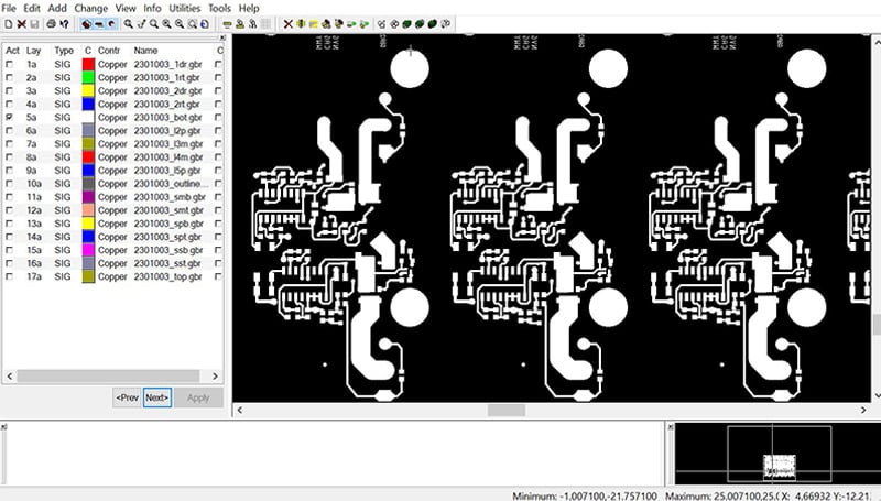
CAD engineering in itself is a specialty process. The engineering team is tasked with developing the tools needed for every process including imaging, plating, drilling, routing, and testing all the required tools needed at each step of the PCB manufacturing process.
Repeated images within an array can save processing time at manufacturing and assembly.
Engineering
Engineering must determine the part/array square inch and location of each part within the master panel including coupons, thieving, text, targets, tooling holes, and optical alignment fiducials. All these items require strategic planning and placement within the usable area. The accuracy from the engineer’s programming skills to determine what is best for production is key for the success of production.
Manipulating the data without risk to the integrity of the PCB and adding processing factors needed to create the end result of quality circuit boards does not come without some risk and the process can be long, depending on the condition of the files received. During data processing, the CAM engineering team will interact directly with our customers to resolve any potential production issues upfront at the initial purchase order placement. The engineer will review all data to determine if there is any missing information needed for production and request by email additional documentation. At the same time, the engineer will also review for any missed steps at the quote level for review with the sales and planning teams.
Production engineering during the initial review for all of the different processes has a pre-determined set of guidelines for engineering to follow for the equipment, chemistries, labs, overage, and time to go. Without the key people in place, the product would not run smoothly, accurately, and on time from start to finish.
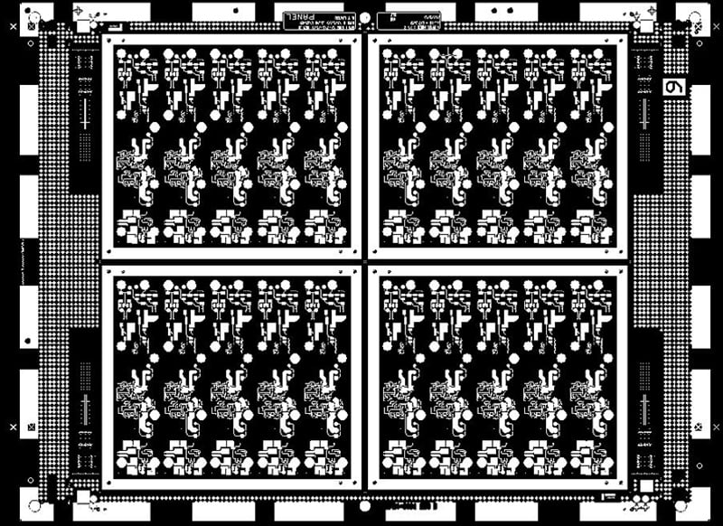
Master tooling includes coupons, tooling holes, targets, thieving, and other production aids.
PCB Production
The engineer must understand the PCB production process to accurately manipulate the database and work with the master panel sizes as defined by manufacturing.
The total size of the PCB laminate includes the individual PCBs and the tooling and waste area. The PCBs we consider the part size or array sizes vs the panel size. The part/array is the format in which the PCB is shipped to our customer. Single pieces or arrays are calculated into the usable space of the master panel. In most cases the usable area is the X,Y of the laminate minus a 1-inch or greater of the perimeter of the master, this one inch can vary for different suppliers or technology requirements.
The calculation of area is, for example, the most common master size of 24 inches by 18 inches, leaving the usable land at 22-inch by 16-inch area. The size of the deliverables is then calculated into the land area left over which equals the panel usage. The ideal piece or array size is 11 x 8 which would fit 4 up on the master panel or 6.5 x 4 would fit 8 times. Those sizes and quantities are optimum for usage. Keeping a higher percentage of used space allows for better cost. When a piece or array is even slightly larger say 11.5 x 8 the used area changed by 50%.
Processing
Understanding the area calculations and usage helps to understand the cost of tooling and panel usage loss. For all areas of production different items are needed to produce the parts. We will review several items needed and why.
Tooling holes for the first example of non-plated or plated holes used for production of the PCBs. They are added to the master panel for different processes to aid manufacturing with the process. For internal layers, holes are punched, pinned, drilled, or routed into the waste area edges for early-stage processing. For registration purposes, these holes are key for front-to-back inner-core imagery. Early stage panels are stacked and pinned for drilling purposes to allow for more than one panel to be drilled at a time. Registration holes, targets, coupons, and first/last drilled holes are placed within the 1-inch production area. These holes are used throughout the process to aid in the manufacturing of the parts, image, layup, mask, legend, drilling, and electrical test all require assistance holes.
Summary
At Epec, we pride ourselves on our longevity in the PCB business with a team of knowledgeable employees that have the experience to produce quality product. We know there are other options out there and we always look to minimize costs for producing PCBs. NRE is always free with online PCB orders placed through InstantPCBQuote.
We will work with our customers on charges, rebates, and reductions whenever possible. For cost savings, always use our free DFM service with real time communication with our engineering team.
Key Takeaways
- NRE charges cover critical setup costs such as data processing, programming, testing, and engineering support to ensure the PCB is manufacturable and meets quality standards.
- DFM review is a vital step, where experienced engineers analyze electronic files, identify errors, and make corrections before production begins, reducing risk and rework.
- CAM engineering creates essential production tools, including imaging, plating, drilling, and testing files, along with features like coupons, fiducials, and tooling holes for accurate manufacturing.
- Panel utilization impacts cost efficiency, as optimizing part/array sizes within the master panel reduces waste and improves yield, directly influencing production costs.
- Tooling aids production accuracy, with strategically placed tooling holes, targets, and registration marks ensuring proper alignment and smooth flow through each stage of PCB fabrication.


