


When it comes to manufacturing printed circuit boards (PCB), providing your PCB supplier with a clean data package can decrease cycle time and ensure requirements are clearly understood.
To assist in this effort, we have compiled a list of the top seven common PCB issues seen during our design for manufacturability (DFM) process that we believe would be helpful for PCB Design Engineers to address.

1. Gerber Files and Mechanical Drawings
First on the list, is the mechanical or fabrication drawing dimensions not matching the actual measured Gerber dimension. We see this discrepancy a lot, where it's stated on the mechanical drawing (usually in Gerber, AutoCAD, or PDF format) and it's stating a dimension from one point to another point, but the actual data (Gerber) that we're fabricating, with measures to a different dimension.
Normally, that's just a documentation error on the mechanical drawing, I'd say, 95% of the time or more the Gerber data is correct, and the mechanical drawing is incorrect. Nonetheless, it can slow you down because on the back end, we have to do a first article inspection. So, when the inspector's measuring the dimensions and they measure it to the drawing, and they mismatch because we built it to the data, then it slows things down.
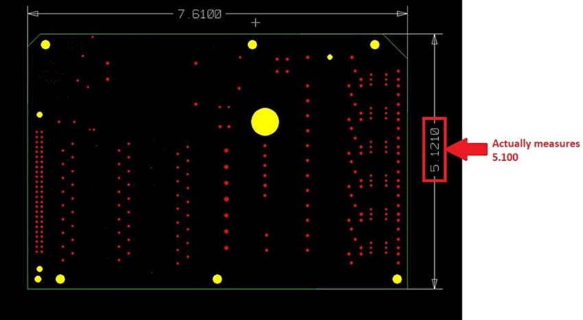
Example of dimensional discrepancy in PCB data file.
2. NC Drill Files and Mechanical Drawings
Similar to the first one, the mechanical fabrication drawing drill chart doesn't match the numeric control (NC) drill files. Often along with a mechanical drawing or fabrication drawing, the customer will put a drill chart saying that there are 10 holes at this diameter, 40 holes at that diameter, and so forth. And what happens is the actual drill data that inputs into the machine, there's a mismatch between the actual data and what is stated to be in the data.
Once again, 95% of the time the NC drill files are correct, and somebody just forgot to update the fabrication or mechanical drawing to match it.
3. PCB Fabrication Notes
The third point is that we see a conflict with specifications, meaning that sometimes we'll see a customer print where they're stating one specification. Maybe they have a master PWB specification, it's a broad-based specification. Then they send us a fabrication drawing, and the two don't align with each other. So, their master specification may say that all circuit boards must have red solder mask, whereas the fabrication drawing references that specification, but goes on to say, we want green solder mask, so we have a conflict there.
The other type of conflict we see with that is they may reference an overall thickness in the fabrication notes stating that the board is to be 0.062” plus or minus 7 mils would be typical, but they also provide us with a stack-up as a separate document, or sometimes contained within the drawing. And that stack-up, when you add all the dielectrics and all the copper weights, exceeds what they're calling out for in the fabrication notes. We believe based on what we've seen is that a lot of customers use a cookie-cutter template when they design enough circuit boards. And instead of typing out their dozen or 50-some odd fabrication notes, however many they may have on their drawing, they notice a pattern as we do. And they cut and paste.
Often when this happens, you are allowing certain things that were unique to one circuit board to now be a specification on another board that doesn't have those criteria. A prime example of a cut and paste would be that one board may have had filled vias, but the next PCB doesn't. We encountered that just today, where the drawing said to fill the vias with a non-conductive via fill, but after looking over the data, there are no vias that are filled with non-conductive via fill, which tells me it's a cut and paste type thing. If you're going to do that, you just need to review each and every one of your notes against the data to verify that the cut and paste that you're applying is applicable to that particular design.
4. Copper Not Specified Correctly
Many customers assume that 1 ounce copper is what we plate, but we don't actually plate 1 ounce. One ounce would be 1.4 mils of copper, but class three would be 1 mil of copper. And that's what's typical. Class II for reference would be 0.8 mil, but I see that often where customers assume or state on their drawing, "Plate the holes 1-ounce copper," and that's a misstatement. It's 1 mil of copper. I'd say that maybe 1% or 2% of the time, they actually do need 1.4 mils of copper in the hole. It's a very rare situation because it's only 1% to 2% of the time that I ever see that, but the times that I see it misstated are far more than the times that it's stated correctly. So as a PCB fabricator, it'd be nice if that were consistent. And that way we know when they put 1.4 mils, they're not misstating something, it's what they actually need.
Often the customer doesn't specify copper weights per each layer properly. The preference would be that they do state the copper weights. One example would be where they have a multi-layer printed circuit board and they say, "Use double-sided, 1-ounce copper," well, it's a multi-layer board, so what are the inner layers?
Another way that I've seen the copper weights misstated is some customers don't realize that inner layers are generally not plated. So, your starting copper is your finished copper, whereas, on your outer layers, we plate those, and so our starting copper is not our finished copper.
I think the easiest way for a customer to specify copper weight is always put it as finished copper weight. Because when we read a drawing, if it's not stated as a finished copper weight, we're unsure, did they intend for us to start with 1 ounce, or did they intend for us to finish at 1 ounce? And so that's the important note there.
5. PCB Fabricator Added Markings
Many customers want traceability. And as a default, we put those types of markings on the printed circuit board, which include a date code, a serial number, even a panel number. So, we know exactly what panel number the boards came off of. But what we would like to see is that the easiest way for us to do it is with silkscreen. We have a machine that works much like a laser jet printer, and the operator, prior to printing the legend ink onto the circuit board, will enter in the appropriate date code, the appropriate panel number, and the appropriate serial number and allow it to print. And the machine is capable to up the sequence for every PCB that it goes to. So, if you start with serial number one, the machine logic is that the very next board is going to be serial number two, serial number three, serial number four.
And so, the point here is that for us to be able to do that, we must do it in the silkscreen. If it's specified to be in the copper etch, we can't do it that way. So ideally, they should allow flexibility on traceability markings, maybe give the fabricator the option to put it in either etch or silkscreen, even though our preference would be to put it in the silkscreen.
6. Material Callouts
I see discrepancies where the print will call out an IPC standard, which is an industry-accepted standard for material, but then they give a brand-specific material, and then the two mismatch and that we don't understand what they want. For instance, an example is the print may state, "We want the material to be per IPC-4101/24," and then they go on to say 370HR, well, 370HR does not meet /24. 370HR would be /98, /99, /101, and /126. So, there is a mismatch within that statement itself, an inconsistency. What we recommend is simply go by the IPC specification. Don't go brand-specific. If there's a reason to go brand-specific, then so be it. Or if you decide that you want to go brand-specific, then allow an equivalent if it's possible.
Different PCB fabricators have different alliances with different material manufacturers. Ours happens to be with Isola but AGC, formerly Nelco, they have a very compatible and good material as well, nothing wrong with their material, it's just no fabricator wants to stock any more material than they have too. So, you pick one and you go with it. And as a customer, it should be allowable if you can provide an equivalent to a particular material, once again, unless there's a very specific requirement.
7. Over Documented Can Lead to Conflicts
The last thing is that there's often reference to the proper IPC standards, and as such, there's many more notes that they're putting on their drawing that are not necessary. If you look at the IPC standard and if you're talking about a typical rigid printed circuit board, the appropriate standard would be IPC-6012. IPC-6012 covers a lot of different things.
It covers... If you say, "I want IPC-6012 class 3," then as a PCB fabricator, we are familiar with that. And we understand that it's going to be a 1-mil plated through-hole with 0.8 mil minimum. And it covers any kind of defects that are allowable in a printed circuit board and what's not allowable. And for the print to restate any of those things can sometimes create a conflict. Now, even within the IPC standard, the order of precedence would be that the print takes precedence over the standard. What I'm finding, though, is that sometimes they'll reference an IPC standard, but what they put in their print would be actually, a lesser stringent requirement, and maybe that's done purposely, but the point is that the simpler you can make your documentation and the fewer notes that are necessary to convey what you need, I think the better off you are at keeping your documentation up-to-date.
The point here is that many of the documentation errors that we see have to do with redundancy of stating the same thing within the document, and as such, if one of those things changes, it must change every location that's referenced within the document. Ideally, just reference it one time, and that way you only have to update it in one location.
Summary
Fabricating and designing printed circuit boards can be a challenge, so we shouldn’t let data discrepancies be a hindrance. Running a DFM is something we do on all PCB orders. Epec also offers a free DFM service, where you can upload your data files ahead of time and our engineers will review to see if there will be any issues prior to manufacturing. We hope these tips will help to eliminate misunderstandings and decrease cycle time, allowing us to deliver faster and better PCBs.
Key Takeaways
- Gerber vs. Drawings Misalignment: Mechanical or fabrication drawings often show dimensions that don’t match the Gerber data, causing inspection delays.
- Drill File Discrepancies: NC drill data usually reflects the correct design, but mismatched drill charts in drawings create confusion and slow quoting or production.
- Conflicting Notes and Specs: Copy-paste errors in fabrication notes (like filled vias or solder mask colors) often conflict with stack-ups or master specs, leading to unnecessary review cycles.
- Copper Weight Misstatements: PCB designers sometimes mislabel copper as “1 oz plated” when it should be specified in finished thickness. This misunderstanding creates ambiguity, especially across inner and outer layers.
- Over-Documentation Risks: Redundant or conflicting references to IPC standards and brand-specific material callouts complicate manufacturing; simplicity and consistency in documentation improve accuracy and turnaround.


