


Flexibility is a critical element in most flexible circuit board designs. Whether it’s to meet a tight “one-time bend-to-fit” application or a “dynamic” infinite bend cycle application. To meet these requirements, a flex circuit design must be kept as thin as practically possible, use the correct copper type, and utilize the correct copper plating process.
The correct combination of these design elements will ensure that the physical properties of the copper circuitry are not exceeded when the flex circuit is put into use. If surpassed, the copper, like any metal, will deform, which in turn will cause embrittlement. If it is then bent again, this will very likely develop cracks in the circuitry.
In this blog, we’ll review the two available plating methodologies: selective pad plating and pattern plating and which is preferred for flexible circuits.

Plating Methods Defined
All circuit designs, either flex or rigid with two or more layers, require a copper plating process to deposit copper with the drilled barrels of vias and plated holes to create the vertical electrical interconnect between layers. To achieve this the industry has developed two methods with the difference being where the copper plating is allowed to be deposited.
Pattern Plating
The original method, pattern plating, is the traditional process used on rigid printed circuits. This technique deposits copper both within the barrels of the vias and plated thru holes (PTH) and on the surface of all circuits present on the external layers. The process involves applying a photo imaged mask on the drilled solid external layer copper surface that defines and exposes all the circuitry, pads, and drilled holes that are to be created. Copper is then plated within the holes and on the surface of all circuits and the unnecessary copper is then subsequently etched away to create the circuitry. This method is cost-effective and meets the requirements of the majority of rigid PCB designs and some unique flex circuit applications.
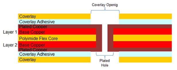
Pattern plating cross section example.

Pattern plating imaging mask example – exposes traces, pads, and hole locations.
Pad Plating
The pad plating process is a variation of pattern plating developed specifically to meet the mechanical bend requirements of flex circuits. This method is a two-step process that utilizes an additional initial image masking process that exposes only a small ring area around each hole location that is to be plated. The parts are then copper plated, but the mask restricts the copper plating to within the barrel of the hole and to a small ring surrounding the holes. After plating the initial image mask is then removed and a second photo imaged mask applied. This second mask defines and protects the circuit pattern and allows the balance of the copper to be etched away to form the final circuit patterns. The finished circuit pattern remains at the thickness of the starting base copper and each plated hole/via is surrounded by a raised copper plated ring slightly thicker than the amount of copper plated within the holes. This ring is necessary to allow for material and manufacturing tolerances as the initial mask cannot overlap the drilled holes.
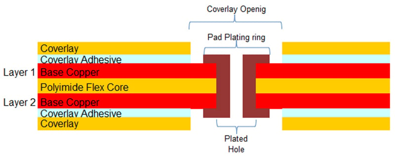
Pad plating cross section.

Example of a primary pad plating mask (only hole locations exposed during process).

Example of secondary imaging mask protecting circuitry during etching process.
Preferred Plating Method for Flex PCBs
The pad plating method is, with few exceptions, the preferred solution for flex circuits for the following reasons:
- Minimizes finished copper thickness for improved flexibility
- Allows for the use of rolled annealed copper
- Improved controlled impedance performance
The copper is both the stiffest material and the critical element within a flex circuit. It creates the electrical interconnects and must withstand the mechanical bend requirements. Minimizing the thickness of the circuitry has the advantage of greater flexibility allowing for tighter and reliable bend radiuses. Exceeding the minimum bend radius of a flex circuit construction is a failure mechanism that results in cracked circuits. Utilizing the pad plating method, the finished circuitry is constructed only of the initial starting base copper on the core material with no added thickness from the plating process.
The second advantage relates to how the pad plating process combines with the type of copper used in a flex circuit. In most designs it is preferred to specify “rolled annealed” (RA) copper. This type of copper is more flexible and mechanically reliable when bent. All copper, for either rigid or flex circuits, starts as plated/electro-deposited (ED) copper, which has a vertically oriented grain structure.
For flex circuit applications, the copper is subjected to a rolling and annealing process. This transforms the vertical ED copper grain structure to a horizontal and elongated structure which increases the flexibility of the copper and provides improved mechanical reliability in tight bend applications. As mentioned, during the manufacturing of a flexible circuit board a plating process is necessary to plate up the vias and PTH holes. At this stage only, ED copper can be applied to the flex circuit. If the ED copper was allowed to be deposited on top of the starting base RA copper, all the mechanical bend and reliability benefits of the RA copper would be negated.
Controlled impedance designs also benefit from the pad plating process. During the copper plating process, when electrical current is applied, “current eddies” form in the production panel. These eddies result in a greater amount of copper being deposited around the perimeter of the panel than at the center. Plating process parameters are set based on the required amount of copper deposited at the center of the panel, to meet IPC specifications, which then results in thicker copper at the panel extents. The difference in copper thickness will vary the impedance values slightly between parts located at the center of the production panel versus parts at the corners. The resulting line widths and spacings from the etching process are also more uniform as the copper is at a consistent thickness across the entire production panel.
Design and Documentation Considerations
The pad plating process adds a couple of requirements both in the design of the circuit and to the documentation.
For the Gerber layout, there is a minimum requirement for the size of the via and PTH pads in relation to the hole size(s) to allow for the pad plating process. This is to specifically allow for the presence of the raised copper-plated ring that surrounds each plated hole. During the application of the photo imaged mask that defines the circuitry the mask must conform over the top of the Pad plated rings that surround each plated hole. As such a minimum of a 0.012” pad diameter oversize, in relation to the hole size, is required to provide enough surrounding pad for the imaging mask to conform and adhere.
With pad plating, combined with the use of RA copper, the copper type must be specified in the documentation in either the drawing notes or in the material stack up. RA copper also has a grain direction which needs to be defined as being oriented in the length of the flex in the area with the tightest bend requirement.
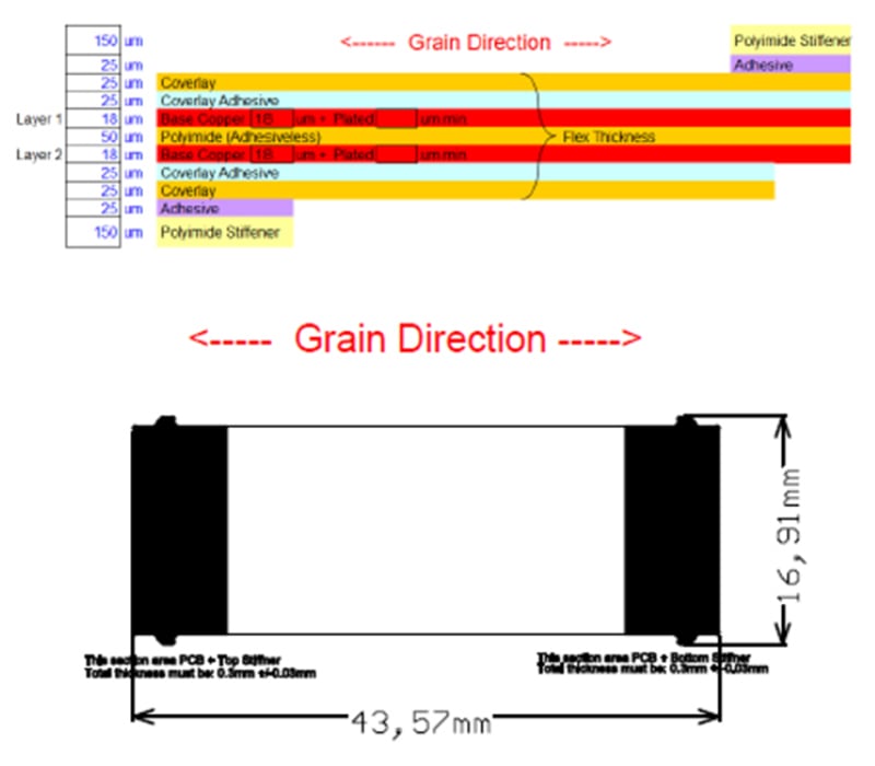
Documentation example RA copper grain direction.
Summary
While both pad and pattern plating methods serve the purpose of depositing copper plating within the barrels of the vias and plated through holes, the pad plating process is the preferred methodology for flex circuits. The benefits are in the improved flexibility and reliability of the finished flex circuit when bent into the required configuration.
This applies to “bend-once-to-fit” applications but is a definitive requirement for a dynamic flex application. Feel free to contact Epec if you have any questions or require support in developing a flex design and specifying the correct plating method to meet your design requirements.
Key Takeaways
- Flex circuits require the correct plating method to maintain flexibility, prevent embrittlement, and ensure reliability under bend conditions.
- Pattern plating adds copper to all exposed circuitry, making it cost-effective for rigid PCBs but less suitable for applications requiring high flexibility.
- Pad plating minimizes added copper thickness, preserving the mechanical benefits of rolled annealed (RA) copper and improving flex circuit performance.
- RA copper combined with pad plating enhances bend reliability and controlled impedance performance by maintaining consistent copper thickness across the panel.
- Proper documentation is critical, including specifying copper type, grain direction, and via-to-pad size requirements to accommodate the pad plating process.


