


When I think of the song, “Through the Years” by Kenny Rogers from 1981 (played at my high school graduation in 1982), I wouldn’t have imagined I would still be in the printed circuit board (PCB) industry. Yes, 1982! Wow. There are several nostalgic “things” about the time spent in the industry that still remind me of my hometown, family, friends, the U.S., my first real job doing something I had never heard of, hoping to make ends meet.
I remember my first thoughts were, “I’m so glad to have a job, and I hope I can find another one soon.” The truth is, the more I got to know the process and the people, the more I liked it. Growing up wasn’t always easy. Working in a factory to make ends meet was hard, hard work, long days, and came with little thanks. But the product, the challenges, the endless hours, plus OT and seeing the final goods was awesome.
One major change in the PCB industry over the years is the circuitry itself. In this blog post, we will discuss the challenges between circuitry and copper weights, the design limitations, and manufacturing challenges in today’s industry standards.

Raw Data vs. Modified Data: What is the Difference?
Understanding the difference is critical to processing, accuracy, and deliverables. Let’s start with what engineering refers to as raw data. What it is, and why it is important? Raw or original files come from an idea to a concept through development and laid out by skilled engineers. The file components are carefully placed, designed, and routed to meet the customer expectation for functionality. Upon receipt by your PCB manufacturer, the files are assumed to be as designed, not modified in any way, and assumed to be what the desired finished PCB should match.
At Epec, we store all customer original supplied data in a secure server that is password protected. The files are as received through email or a secure link and downloaded, stored as a permanent record linked to our customer and part number in a folder labeled “original.”
Modified data (files) is another challenge. Often, customers lose track of original files and where they are stored, or have improper containment, leaving only modified for process files accessible. It is a problem and costly to fix. No one wants to add design and layout to a PCB that has already been made; how do you explain that cost?
Our engineers are trained to look for modified data. We look at the original zip file received for items like file naming conventions used, dates, UL/DC adds to copper or legend, or data that has been clipped or modified from what would be original. Files that are stepped up into an array layout with adds or removal of data are also clues to non-original raw files.
Truly, the modification indicators are clues that the files have been modified, there is no actual way to identify all the modifications that have been made to the files, leaving your fabricator in the dark.
Circuitry and Spacing
At the layout stage, circuits and space are defined by embedded code, aperture listings. The apertures show, size, shape, location, net, beginning, and ends. Where the nets link and to what layers they link are also within the data. Data as defined within the originals should always be desired finish in reference to the IPC-6012 latest revision. Example: 0.005” circuit and 0.005” space should be what is desired for finished circuit and space.
When circuitry is changed, increased, or decreased the original defined width is unknown. The same goes for pads, shapes, and sizes. When the CAD data is modified, saved, and exported, the changes are now defined by a new aperture list or embedded code. It has a new size, shape, and location. Change is necessary for production, however losing originals can be detrimental.
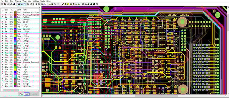
Example of critical spacing vs. copper.
Why Do We Modify PCB Data?
The answer is rather simple: for processing.
The build of a PCB is a process. In fact, it’s many, many processes. For starters, back to CAM, files are reviewed, a DFM is performed (always free at Epec), originals are saved, archived, and stored. An exact duplicate is used to produce manufacturing files. After the initial clean up, files are modified.
Adjustments are made to circuit widths, decreasing spacing. Pads are also considered for increase length, width, or both. In making these small changes we allow for processing loss. For example, a 0.005” circuit will increase to 0.0055” or 0.00575” or 0.006”, depending on the copper weight. By increasing the features, manufacturing can now process the PCB. After each process, in this case etching the files will return to 0.005”. We call this the addition of an etch factor.
What is Etch Factor?
As defined by PCB manufacturing, the etch factor is a modification of data or compensation to allow for the chemical etching process of the PCB. It is a process where internal copper layer and external copper have non-circuitry copper removed from the laminate surface, leaving behind only circuitry as defined in the database.
Etch factor is considered when the copper thickness for each individual layer is defined. Standard copper weights are 0.5, 1.0, and 2.0 ounces; 3, 4, and 5 ounces are less common, however, they are used frequently.
The copper considered will drive the modification to prevent loss beyond functionality. Considering copper weight needed at the design level, allowing for greater spacing, will create ease of manufacturing challenges.
Example: 0.005” space with 0.005” trace, when increasing for a 0.5 oz copper the traces are increased by 0.001.” When traces are bundled together in groups, the spacing becomes 0.004”, and the traces become 0.006”, allowing for an etch factor of 0.001” loss. This is extremely doable. However, thicker copper poses a problem. Using the same example of 0.005”/0.005”, imagine on a 1-ounce copper, twice as thick to etch through.
The same files have a greater etch factor needed to etch through the thickness to the laminate below. Modifying the 0.005” circuits to 0.0065”, 0.00675”, or 0.007” will be needed to compensate for the loss. This compensation, for 1 ounce is too great for the spacing causing too much loss of space; 0.005” circuits modified to 0.0065” for 1 ounce will leave a space of 0.003” to etch through to the surface laminate.
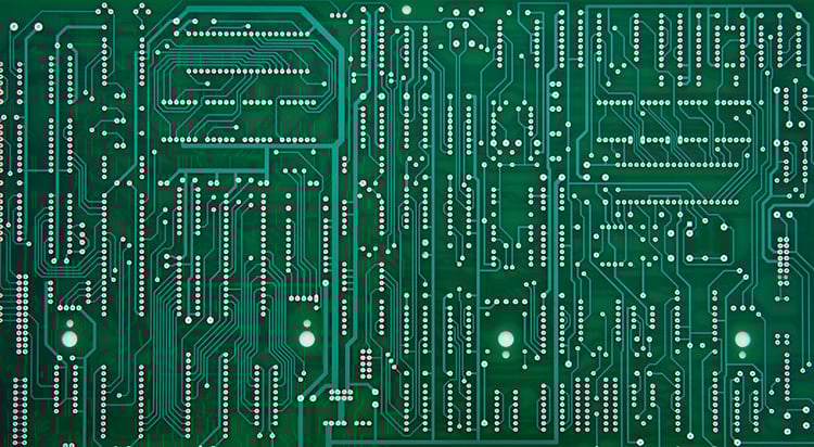
Example of how PCB circuitry has changed considerably over the years.
Copper, Line Width, and Spacing Considerations
The standard rule of thumb is to consider the copper ounce first to aide in compensation needed for production. Some basic guidelines are: 0.5 ounce will need 0.001” increase; 1 ounce will need 0.0015” - 0.002” increase; 2 ounces will need 0.0025” - 0.003” increase, and so on. The thicker the copper surface, the more compensation or etch factor is needed.
For example: 1-ounce material, and the desire line with is 0.005”, increase the space to 0.006”, the greater the ounce the more space is needed to aide production in compensation.
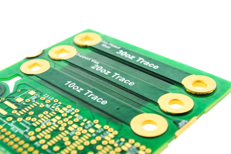
Multiple copper weights on the same layer of circuitry.
Summary
We encourage you to know more about the important items like etch factor, copper weights and circuit design. It is critical to our processing success. Involve an engineer at the fabrication level using Epec’s free DFM service. At Epec, we welcome our customers to ask questions and use our team to help in your successful designs.
Key Takeaways
- Raw vs. Modified Data Matters: PCB manufacturers need the original unmodified design files to ensure accuracy. Modified files often include processing adjustments and can complicate troubleshooting or redesign efforts.
- Etch Factor Compensates for Processing Loss: Line widths are intentionally increased during data prep to account for copper loss during etching. This “etch factor” adjustment ensures final circuitry matches the intended design.
- Copper Thickness Directly Impacts Spacing and Line Width: Heavier copper requires larger adjustments. For instance, 0.5 oz copper typically needs a 0.001” increase in trace width, while 1 oz may need 0.0015” – 0.002”, and 2 oz can require 0.0025” – 0.003”.
- Tighter Designs Are More Challenging with Thicker Copper: Fine-pitch traces and minimal spacing become increasingly difficult to maintain when using thicker copper, making early design planning essential for manufacturability.
- Early DFM Review Prevents Issues: Engaging your PCB fabricator early in the design phase allows for guidance on copper weight, line width, and spacing requirements, avoiding costly revisions and manufacturing problems.


