


You may be asking: what is an HDI printed circuit board and what makes it different than standard PCBs? Let’s break it down for better understanding from a design and from a supplier point of view. As Epec continues to grow our design business, it has become very apparent that many designers are very good at what they do and have no manufacturing knowledge to proof designs against.
As I am writing, I think of the movie Field of Dreams with its famous line: “If you build it, they will come.” It makes me think, if you design it, it can be built. That is not true, at least not in some cases for sure. So, what is a high-density interconnect printed circuit board? Simply put, it is a PCB that has multiple layers, may contain blind/buried/stacked vias, micro-vias that are <0.008” in diameter, and can use a via-in-pad specialty process. The circuitry is typically <0.005” with a space of 0.005” or less as well. The vias can be from top to mid, bottom to mid, mid to mid layers as well as through vias.

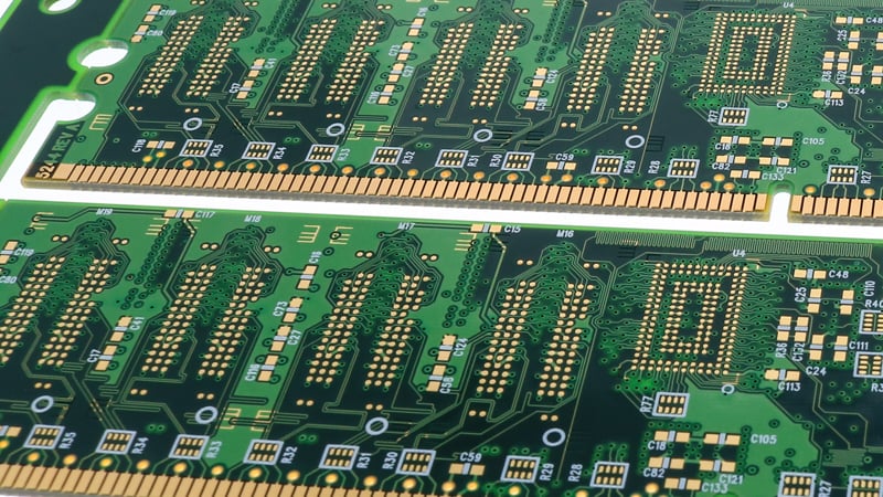
Example of high-density multi-layer PCB.
With all these via types used in a single PCB, the additional steps to process through drilling, plating, and multiple lamination cycles, what do you need to know about the process? The biggest factor is time: the several loops through production to create the proper connecting layers of circuitry take time and in some cases many days of additional processing. During the PCB design phase, limiting the multiple sets of buried vias and the to and from layers aids in time. Pushing blind vias to the top or the bottom also helps in processing time.
Additional copper layers to limit via processing can decrease cost. From a supplier point of view, the many sets of vias increase the time to produce, ties up equipment and resources, as well as increase the risk of fallout.
Designing PCBs Within Manufacturing Capabilities
For every via step, there is an equal plating process. The engineering time alone for a processing plan can include a multistep traveler to loop the part through the processing of imaging, drilling, plating, laminating, and repeat. Take the below stack-up for example. As you can see, there are holes from 1-2, 17-18, 2-17, and 1-18 this is 4 trips through drilling, one of the highest costs for PCB processing. Using an additional layer may have omitted the blind vias from the top or bottom side.
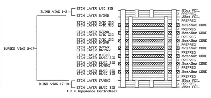
Example of a PCB stack-up with blind vias.
PCB Design Tips
A few tips to consider for design that will ease PCB manufacturing are items like mentioned above, adding copper layers to remove blind/buried via sets. Maintain a balanced copper construction from side to side of the core. In the example above all copper is at 0.5oz this is ideal for processing.
Also, include in the balance, use like layers, signals against signals, ground to ground, if it is not possible and a signal needs to be against a ground or power layer then stagger the book, so the layers are mirrored from the center core outwards.
In this stack-up, the grounds are 2 & 17, 5 & 14, 8 & 11, and power planes 9 & 10. The mirrored symmetrical build balances the copper pour to aid in the warping and twisting of the PCB. When in the design phase, review component availability and lead time and if there are any other options or crosses that can be used. Review hole sizes and their tolerances and combine holes that are within .001 of each other when it makes sense.
Avoid necking down circuits in troubled areas and when it is unavoidable note the change location for production. Bundled circuits can pose a problem when adding etch compensation to data, allow for proper spacing in the design, and don’t trap bundles in via land areas nearby. Utilizing the top and bottom sides for component placement is typical and, in most cases, unavoidable. However, one final tip to consider is space, the space available in your product for the PCB to rest. Increasing land is our final tip for making the impossible possible. Adding length and or width to the PCB size allows for additional routing, spacing, and through vias. When you consider the circuit and space of 0.005”/0.005” and add 0.200” to the LxW it may seem minimal, but routing can make all the difference in the final part.
Summary
HDI PCBs are distinct from standard PCBs due to their multiple layers, the inclusion of blind/buried/stacked vias, micro-vias with a diameter <0.008", and the ability to use a via-in-pad specialty process. The circuitry in HDI PCBs is typically very dense, with traces and spaces both <0.005". The use of various via types in a single PCB requires additional steps such as drilling, plating, and multiple lamination cycles, making the manufacturing process more complex and time-consuming.
PCB designers need to be aware of these manufacturing complexities and consider design choices that reduce processing time, such as limiting the use of buried vias and carefully planning the via placement. Adding copper layers and maintaining balanced copper construction can also improve manufacturability. Moreover, designers should consider component availability, lead time, hole sizes, and proper spacing in the design phase.
Watch Our Video
Ensuring Consistent Hole Plating when Dealing with Aspect Ratios
Key Takeaways
- HDI PCBs Require Precision and Complexity: High-density interconnect PCBs involve multiple layers, micro-vias (<0.008”), via-in-pad processing, and tight trace/space requirements (<0.005”), making them more complex and time-intensive to manufacture than standard PCBs.
- Each Via Structure Adds Significant Manufacturing Time: Every blind, buried, or stacked via demands an individual cycle of drilling, plating, and lamination. Reducing the number of unique via layer pairs in the design helps lower cost and production time.
- Balanced Stack-Ups Improve Yield: Symmetrical builds with mirrored copper weights and like-layer pairings (signal-to-signal, ground-to-ground) reduce the risk of warping and improve reliability during high-density fabrication.
- Strategic Layer Count Can Reduce Via Complexity: Sometimes adding a copper layer allows you to eliminate blind vias, improving manufacturability and reducing processing loops, saving both time and cost.
- Allow Extra PCB Real Estate When Possible: Expanding the PCB’s length or width slightly can make room for more efficient routing and through vias, especially important when working with tight 0.005"/0.005" trace and space geometries.


