


There are several reasons for the need to plug printed circuit board (PCB) holes. Some of the most commonly seen reasons include properly tenting or covering the via with solder mask (isolation), to prevent entrapment (solder, chemistry, flux), to prevent solder starvation (wicking of solder in the hole/surface mount technology (SMT) placement directly on via), and for thermal or electrical purposes.
The latter two reasons are often referred to as via-in-pad or via-in-pad plated over, and the key distinction between the two is whether or not a cap plate of copper is required over the filled via. If you don’t need to solder directly to the filled via, then via-in-pad is usually adequate.

Via-In-Pad or Via-In-Pad Plated Over
For many years, the need for via-in-pad or via-in-pad plated over was not needed, and as such, via holes could be plugged with a solder mask or plugging mask. As component packages became more complex, preventing solder starvation (as well as for thermal or electrical purposes), came into play and that changed how vias are normally plugged today. As the via-in-pad and via-in-pad plated over process meet the needs of all the previously mentioned reasons, we will just focus on those two processes.
Our process to fill vias, consists of the following steps:
- Drill the holes
- Desmear and electroless copper
- Copper plate the holes to specification, usually 1 mil
- Fill the holes
- Planarize flush to panel surfaces
- Cap plates with copper (only if via-in-pad are plated over)
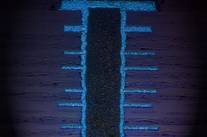
Example of a PCB filled Via cross section.
Drill Process
The diameter range of holes that can be filled depends upon the overall thickness of the PCB. For discussion purposes, we will assume it’s a nominal 0.062” thick PCB. The largest hole that you want to plug is 0.028” (2:1 aspect ratio). If you get larger than that, it's very difficult not to have significant voiding in the via fill. The smallest diameter is 6 mils (10:1 aspect ratio), which after plating, you are filling a 0.004” hole, and this can be difficult to do. Normally, we see them fall in the range of 0.008” to 0.012” (5~8:1 aspect ratio is ideal).
Video: Lenz DLG-550 in Action: High-Speed, High-Accuracy PCB Drilling
Desmear/Electroless Copper Process
A desmear process slightly attacks or removes epoxy. And it is a common process run on any plated through-hole drilled in FR4. Other materials may get different treatments, but desmear is a common process for smear removal, which is epoxy. Regarding a filled hole, it is used to prep the top and bottom surfaces for electroless copper.
Electrolytic Copper Plates
To build up copper thickness to meet plated through-hole specifications, the holes are electroplated with copper. This can be selectively plated to the holes by using a dry film resist on the surface or it can be plated on the entire panel. Usually, it is a combination of the two processes as there would be too much copper on the PCB surfaces if wholly done as a panel plate.
How Holes are Filled
It's different from manufacturer to manufacturer. If you don't have the capital equipment, the way that you would fill it is by screen print. Probably about a decade back, that's how we used to do it. And then we invested in a more automated way of doing it and a better way of filling it, which is a pneumatic fill.
It's gasketed, and it doesn't allow the introduction of air into the process. We take a tube of non-conductive epoxy, and it pneumatically presses through the holes. This process can also be done while under vacuum but is usually not necessary for filling through vias.
Flatness and the Planarize Process
What's key here is the non-conductive via fill height relative to the copper surface. The terminology used for that is one of two things: a dimple or depression. A dimple is where the non-conductive via fill exceeds the height of the copper. A depression is where the non-conductive via fill has a slight recession below the copper.
In IPC-6012, 6018, they address this all, as to what would be acceptable versus what's not acceptable. Very rarely do we see dimples; the more common encounter would be a slight depression, and the allowable amount is up to 3 mils of depression. And if via-in-pad plated over is required, we would plate over the via fill with copper.
Summary
Should your circuit board design require filled vias, it is important that you communicate the following information to the PCB fabricator. Let them know specifically which diameter(s) require to be filled, find out if they are to be non-conductive or conductive fill (the most common is non-conductive, and also be aware that conductive filled vias get very expensive). The product we use 95% of the time is Sanei PHP-900 IR10F. Also, find out: do they require cap plating.
Epec offers a variety of printed circuit board manufacturing solutions for plug via process requirements, whether you require vias flooded with mask, selective plugging in BGA areas, conductive and non-conductive epoxy fill, copper filled, or fully plugged and via-in-pad. Our experienced engineering team will help you to get your product to market faster and help to eliminate delays and quality issues.
Key Takeaways
- Via-in-pad techniques are essential for modern PCB designs: As components get smaller and more complex, via-in-pad and via-in-pad plated over methods help prevent solder starvation, improve thermal/electrical performance, and reduce signal integrity issues.
- Hole size and board thickness determine fill success: The ideal aspect ratio for via filling is between 5:1 and 8:1. Holes larger than 0.028" or smaller than 6 mils can be challenging to fill without voids or failure during operation.
- Modern fill processes improve reliability and consistency: While screen printing was once standard, pneumatic fill systems now allow for more precise and uniform epoxy application, critical for high-reliability PCBs.
- Planarization and fill quality affect solderability: Achieving the correct flatness after via filling is crucial. IPC standards allow for up to a 3-mil depression, but consistency ensures successful plating and reliable solder joints.
- Clear communication with your PCB fabricator is critical: Always specify hole diameters, type of fill (conductive or non-conductive), and whether cap plating is needed. These details help avoid costly errors and ensure manufacturing success.


