


In 1913, the comic strip (which then led to the phrase of the same name) “Keeping Up with the Joneses” was brought to life in print. Although that comic strip ended in 1940, let’s face it, in every aspect of the phrase, it is still in practice today. In business and as consumers, we look ahead to what is next. From a freshly opened new cell phone or television, we are already counting the days until the next rendition is available.
It matters to us how big or small a product is, or what it can or cannot do that are most important. Performance and outdoing our neighbors, the Joneses, is what drives our products and processing changes to make them outperform their prior version, or better yet, the competition.

Why Was Via-in-Pad Developed?
Space. That is the simplest answer. We are living in the Jetsons’ age. The future that Hanna-Barbera dreamed of is here (minus the flying cars but stay tuned). Quick prep ovens, microwaves, cordless phones, computers were all predicted then.
As we push the technology limits, processing printed circuit boards has developed into somewhat of a trial and error to accommodate engineers’ dreams to do more with less space.
A great example to walk through is to look at all the types of cellular phones on the market. Think about it: the initial cordless phone was as large as your landline phone, and they had a pullout antenna. Quickly, the consumer pushed for a smaller, all-inclusive handheld size, smaller, yet to fit in your pocket for easy access. And at the same time, we wanted our phones to do even more, such as acting like calculators, take notes, record audio, take and store photos, have the ability to make conference calls, etc. The list goes on.
As PCB designers increased the functionality, the number of layers used within the design increases. Even with the components placed on both sides, blind vias and buried vias still did not allow for enough surface space for all of the components to be placed. Component footprints increased as we strived for them to do more. We need vias to pass current from layer to layer but with lack of land where and how?
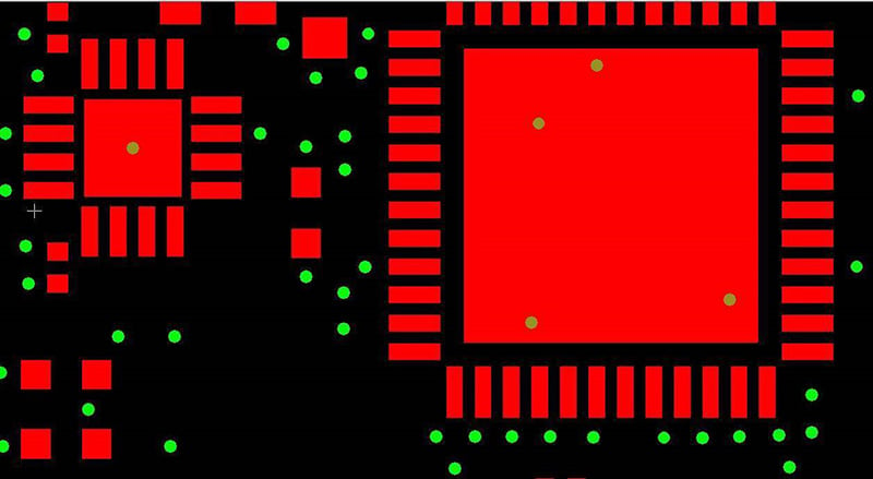
The green within the red are the vias within the pad. These would be filled with epoxy, sanded down, and plated over, invisible to the eye.
Where Can We Place the Pesky Via?
Someone had the idea to place vias in the component lands, CAPS, resistors, quad-flat packs, suddenly had holes through them it was the beginning of yet another PCB manufacturing challenge. I am sure a lot of thought went into this idea just as sure as I am that there was just a little thought into how we were going to process them.
Oddly enough, the challenge was met. Seeing that the via still had copper around it, drill and plate them and move on, until these little devils started to cause problems at the assembly stage. As these carefully placed vias robbed components of paste and solder component placement was challenging. The vias would need to be filled and the surface would need to be flat to solder as well.
Standard processing equipment could not be used. There were plenty of ideas on how to achieve what was needed, but still the challenge would be how. For a long time, vias had been secondary processed in solder mask with a plug applied to one side or both. This process could not be used on the solderable surface.
Example of vias within a printed circuit board design.
Conductive vs. Non-Conductive Via Fill
Non-conductive via fill, for via-in-pad, is an epoxy fill. While the via walls have copper and are complete, they still need to be filled. With the use of squeegee and vacuum suction the liquid is applied to the surface and pulled through the via, and the content is cured inside the hole. The same process is followed for conductive required filled holes are processed the same only the epoxy contains a conductive component, such as silver.
In the via-in-pad process, most often the vias are filled with a non-conductive epoxy, cured planarized down to flatness to meet the board surface and cap plated. The via still electrically sound is now part of the component land. There are also conductive fills available if heat dissipation is a concern, and these epoxies are applied the same the only difference is they contain silver or other conductive matter.

Summary
The benefits for via-in-pad were great. Circuit board manufactured with this technology had fewer layers, increase land for routing, heat reduction for components, and a better surface to bond, too. The process itself has come a long way as the increased technology has been used. Smaller ball grid arrays (BGAs), tighter pitch surface-mount devices (SMDs), reduction in density without losing functionality are just a few reasons why we love this technology.
If you go back to my original example, the cordless phone and the evolution of it, you most likely have had several yourselves. The slide phone or flip phone have both internal antennas and the use of flex circuits. The iPhone and its new version with multiple cameras and the many variations of sizes are all possible due to technologies that have been developed to process the PCB inside. Not that all these wonderful technologies have stopped developing, but we sure have come a long way.
Key Takeaways
- Origin of Via-in-Pad: Developed to save board space as component density increased, especially with smaller, high-functionality devices like cell phones and BGAs.
- Processing Challenge: Standard solder mask plugging methods were insufficient, as open vias in pads caused solder wicking and poor component placement, requiring flat filled vias.
- Non-Conductive vs. Conductive Fill: Most via-in-pad holes are filled with non-conductive epoxy and plated over, but conductive fills with silver or similar materials are used when heat dissipation is a concern.
- Benefits of Via-in-Pad: Enables fewer PCB layers, more routing land, improved heat reduction, and reliable soldering surfaces for fine-pitch components.
- Modern Applications: Common in advanced electronics with tight layouts and small packages, this technology supports smaller, faster, and more reliable products.


