


When talking about the design and manufacturing of printed circuit boards (PCBs), customers mainly focus on the controls and signal frequencies that the PCB will perform for the specific application. Another topic to also take into consideration is the insertion loss.
Insertion loss occurs when there is a loss in the signal's strength or power when passing through components, systems, and materials. This issue may also be referred to as attenuation when discussing the power loss within the length of a transmission line. Improving the insertion loss during the PCB stack-up ensures that the application will operate within specifications when receiving higher signals of 10Ghz to 30Ghz or more.

What Causes Insertion Loss?
There are three main causes of insertion loss: copper losses, dielectric losses, and reflected losses. These losses are measured in decibels and is represented as a positive number.
- Copper losses: Copper losses occur when the connector's conducting surfaces cause the power to become dissipated. This problem is usually the result of the plating and the material that is used in the PCB.
- Dielectric losses: Dielectric losses occur when the dielectric materials used in the PCB layers cause the power to be dissipated.
- Reflective losses: Reflective losses occur with the connector's voltage standing wave ratio (VSWR) when in transmission lines. It occurs when the power does not become accepted by the load, as it becomes reflected back along the line.
For PCBs using lower speed rates, such as 3Ghz up to 5Ghz, a mismatch in impedance usually results in signal loss. Yet, with the higher speeds of 10Ghz to 30Ghz+, the materials used to create the dielectric constant will be the top issue that could be creating the insertion loss. To deal with these many issues, selecting the appropriate materials for the core, prepeg, and copper foil becomes essential when building the PCB stack-up.
Various printed circuit board material manufacturers.
PCB Material Stack-ups
High-speed PCBs will have multiple layers of materials, as each layer will have a specific thickness and width. There will be alternating layers of core and prepeg with copper clad foils that will be bonded on both sides of the core materials. The internal copper foil layers will act as the signals and planes of the PCB.
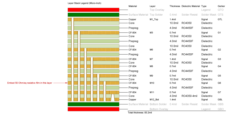
Example of a PCB material stack-up with alternating layers of core and prepeg.
The cores will provide the insulation needed to isolate the signals between the copper foils as they will consist of common dielectric materials such as FR-4, polyimide, thermoset hydrocarbon or PTFE laminates with a fiberglass/ceramic weave. The prepeg acts as the glue that will hold all the core materials together in the multilayer PCBs; it is commonly fiberglass-epoxy woven weave that is uncured. It also functions as an insulating layer between each core layer.
When it comes to dealing with insertion loss, many factors concerning the lamination thickness, copper foil selection and width, and even the glass weave can have an impact with how much of the signal frequency is transmitted and received in the PCB. Minor to major variations can improve this loss, based on how much of the signal that needs to reach the end of the transmission line. To lower and mitigate signal loss, four parameters need to be addressed when selecting the appropriate materials and specifications: skin effect, fiberglass weave composition, relative dielectric constant, and loss tangent.
Skin Effect
Skin effect is a parameter that focuses on how much resistance there is within a channel that causes the signal frequency to be absorbed. Signal loss can happen when there are resistive losses in the channel that flows through the copper.
Think of this flow much like a river of water with the copper plane acting as the banks directing where the signal is going. When there is a lower level of signal frequency along the channel, it will flow throughout the copper foil. Yet, when higher frequencies are introduced, the signal becomes concentrated at the surface of the copper trace. There is less cross-sectional area available along the channel as there is more resistance that leads to skin effect and insertion loss.
To tackle this issue, many customers believe that increasing the thickness of the copper will provide more cross-sectional area for the signal frequency. Yet, as we mentioned, the higher frequencies will move to the surface and become concentrated. The weight of the copper foil no longer matters. Instead, increasing the width of the copper foil traces allows for an increase to surface area, lowering resistive losses.
The roughness of the copper also has a significant impact on insertion loss for the PCBs. The copper foil does not have a smooth surface, as this helps with the lamination and bonding processes. In addition, the rough surface increases the electrical rates and peel strength. However, the roughness of the copper can cause uneven current flows along the fields, resulting in insertion loss. To address this problem, your material selection will need to focus on low profile copper or very low profile electrodeposited (ED) copper to use for PCB foils. In addition, avoiding black oxide processes can also be a benefit to controlling the roughness of the copper foil. Using alternative oxide before the lamination process is suitable.
Fiberglass Weave Composition
The core and the prepeg materials will consist of woven glass yarn fibers, which will look very similar to a fabric-like sheet as it will then be impregnated with the cured and non-cured resin. This glass yarn will have different thicknesses as well as densities, as there may be very tight weaving or very loose weaves. The copper traces will then be routed across the weave.
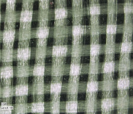
Example of woven glass yarn fibers.
Source: https://www.isola-group.com/wp-content/uploads/Understanding-Glass-Fabric.pdf
When the fiberglass weave is tight, the dielectric constant is more uniform with less impedance. So, it stands to reason to always select materials that have a tight weave. However, cost considerations for the application can force a customer to select a fiberglass weave that is looser. This looser weave will cause some of the traces to be on the weave and some of them to be off the weave and on the resin itself. In these situations, placing the copper traces in a straight line will result in variations in impedance as well as propagation skews because there may be more off-weave traces than on-weave traces. Instead, placing the copper traces on an angle or zig zag design can even the on/off weave traces for better dielectric constants.
Relative Dielectric Constant
Every core layer material and laminated material has varying dielectric constants. This dielectric constant is a measurement to see how much potential electrical energy the material will possess and how much it will interact or impact signal frequencies. In addition, the dielectric constant can change based on the signal frequency that is introduced, as higher frequencies will require the materials to have more even dielectric constants while standing up to the increase in temperatures.
Insertion loss will usually occur because the PCB will be receiving multiple frequencies from the sent signals. Due to the different frequencies, differing impedance is present from the material, which can result in some of the signals becoming reflected or to experience phase distortion. Selecting a material that possesses a lower dielectric constant that has a flat frequency response is ideal as you want a material that provides faster signal propagation, smaller stray trace capacitance, and has a more consistent electrical energy to differing signal frequencies.
Loss Tangent
If the dielectric materials significantly absorb the signal, it means less of the frequency is reaching the desired end destination. For transmission lines in transceiver-based designs, this signal loss is also called the dissipation factor, as the materials will have an electromagnetic wave absorption rate.
The ideal material to use to deal with the dissipation factor is a low loss material so that more of the transmitted signal can pass through the transmission line with resistance, reflection or absorption. Lower loss materials will have greater costs, which can seriously impact the production of the PCB's stack-up.
How to Improve Insertion Loss
Dealing with insertion loss can help you design the right high-speed PCB for your application. By understanding the main issues that create this signal loss, you can decide on the types of materials to use for the stack-up, the weave of the glass and resin density, and the thickness of the PCB. To recap on this topic, things to take into consideration for your PCB stack-up include:
- Minimize skin effect and surface roughness of the copper foil by selecting low profile copper, very low-profile ED copper and alternative oxide.
- Select tighter fiberglass weaves for better dielectric constants or angle and zig-zag the copper traces over looser weaves for signal integrity.
- Choose materials with low dielectric constants and flat frequency responses to handle the multiple signals.
- Use the lowest loss dielectric materials, as well as shorter reaches, to deal with dissipation factors.
Documenting Material Requirements on PCB Fabrication Drawings
To address all the previously mentioned issues and to inform the PCB fabricator of your material selections for the PCB stack-up, you should include notes with the fabrication drawings. These notes can focus on copper plate thickness, material requirements, etchback requirements, and other specifications. The notes are considered callouts. They will be numbered as the corresponding number will be placed on the PCB fabrication drawings in the designated item location. So, the fabricator can refer to the callout notes for more exact details. In addition, there should be a board layer stack legend that will provide details regarding the layer, thickness, dielectric material, type and Gerber of the PCB stack.

Summary
Speaking directly with the circuit board fabricator will allow you to learn more about what is needed in documentation for the PCB stack-up. It also helps the fabricator to further drill down regarding the requirements of the application. They can make suggestions and recommendations that are more suitable to your application while still being based on the drawings provided .
Key Takeaways
- Material Choice Is Critical: Selecting low-loss dielectric materials with flat frequency response and low dielectric constants is essential for minimizing insertion loss at high frequencies (10–30 GHz+).
- Copper Characteristics Matter: Use low-profile or very low-profile electrodeposited copper to reduce surface roughness and resistive losses. Wider copper traces help more than thicker copper due to the skin effect at higher frequencies.
- Fiberglass Weave Impacts Signal Integrity: Tight weaves offer more uniform dielectric properties. For looser weaves, angling or zig-zagging traces can help balance dielectric constant variations.
- Address Multiple Loss Factors: Insertion loss is influenced by skin effect, fiberglass weave, dielectric constant, and loss tangent, all should be optimized in the stack-up design.
- Document Your Stack-Up Clearly: Use fabrication drawing callouts and stack-up legends to specify copper thickness, material types, etchback needs, and dielectric layers to ensure accurate manufacturing and performance.


