


As printed circuit board (PCB) technology has been on a steady incline for many years, the main focus has been on what else can we make this part do. Add more layers, decrease circuit widths, add more components, buried vias, blind vias, control the impedance – the list of changes in technology is lengthy. As a manufacturer of PCBs, we see the finished design ready to go to production, but is it? Often, we look at a received customer data production and think, “can this part be produced?”
We push the limits of equipment and materials, tweak the process to improve yield, and celebrate the successes. But how has this affected the testing portion of production? The days of optional bare board testing is a thing of the past. No longer can you visually inspect in process or perform an acceptable quality level (AQL) and be confident that the part is good. Have we considered the testing process? PCB designers can impact lead time to process greatly with technology driven PCBs. The more layers, holes, and components, the longer the lead time to process but also the longer it will take to test the end-product. How?
In this blog post, we will review some of the most common types of circuit board testing, the impact on the overall integrity of the PCBs, and the lead time associated with some more advanced testing processes.

Why a DFM Review is Important to Testing PCBs
Electrical test integrity starts with a good design, a clean data set in an RS274X – X2 format or ODB++, and always includes NETLIST data. Testing products start in CAM with design for manufacturing review. Quality data that includes netlist will improve the process.
Testing of PCBs starts in CAM. Engineering performs a basic set up and design review, what we call a “look” at the layers for anything we may “see” as less than standard. When NETLIST is provided, we compare the files to the NETLIST. This is your first test of the future end-product. Engineering will repeat this process throughout the CAMing of the job.
What if we do not have a NETLIST? You would be surprised at how common this is. In fact, it is more common to not have a NETLIST provided. We typically ask our customers if they have one, and most of the time they do not. Our software allows us to extract a NETLIST from the database. This is a good tool; however, it is only as good as the supplied data. If there is an error built within the files and we do not see it or find it in a DFM, the part will process incorrectly.
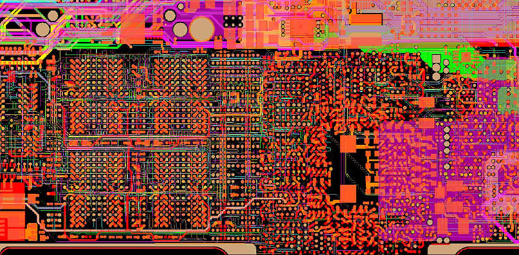
A 2-layer circuit board showing signal layers.
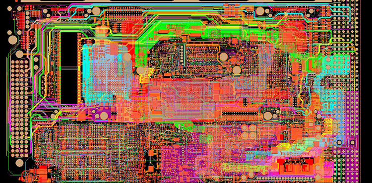
A multi-layer circuit board showing signal layers.
AOI – Automated Optical Inspection
Although this is not an electrical test (ET), it is worth a mention as it is a critical process to a successful build and better yield. Earlier, I mentioned visual inspection is obsolete, the technology level of PCBs is just too great to see the defects. AOI is basically an automated optical or visual inspection. The AOI is downloaded with the electronic data of the layer being reviewed. Using cameras, any discrepancy is recorded with an ink mark for the operator to verify. Catastrophic failures such as missing circuits or breaks or minor defects like a nick or pinhole are also recorded. The AOI is an amazing piece of equipment that has aided in the success of complex board production.
Processing Why Testing Circuit Boards is Necessary
We are often asked, “Do you test our boards or do you 100% test?” The answer is, yes. All orders are electrically tested and all technologies. Some customers believe it or not do not require testing or want the part tested. This is not an option allowed by Epec without some understanding between us and our customers.
Processing high technology or any technology PCB is not an exact science performed solely by machines or robots in most factory settings. It is still throughout most of the industry production lines, manual labor and equipment that is not automated.
Handling materials, equipment failures, chemistries, and human error can all impact processing and cause failures in the circuitry layers.
Electrical Test Time for Advanced PCB Processes
Once the part has completed processing and is in its final ship format, single pieces, or array layout, some ship in a larger panel form, the final product is electrically tested. Often ET is not considered at all by designers or even by PCB manufacturers. Why is this? Well, there are several reasons. With technology increasing, layer count, blind vias, components all add time. Each electrical connection has a start and end point. Some circuits jump from layer to layer using vias as their passageway to the end point. Mid-points in circuitry are plenty full as well as test points (TP) that are placed for end-product testing once assembled. All the examples must be tested, the more there are the longer the test can take.
We estimate the ET time using only what we know, quantity of vias, single sided, or double-sided component placement, the number of through holes, blind holes, or buried holes. From these numbers, we can only calculate what we believe the test time will be.
Testing equipment varies. In most facilities, the flying probe, bed of nails, or clam shell are commonly in place. Bed of nails testers are the traditional or original testing method. Using a bed of nails tester requires a customer build fixture containing, plexiglass layers, standoff pins, holes drilled through the layers to support pogo pins. Typically, a known good board that has passed is kept with the fixture to test the parts against. The area needed to store the fixture is a problem, the fixtures are not small and take up valuable space but are necessary to keep. This is not the desired test method for higher technology today, but it is still used.
Flying probe or probe-bot testing is an electronic method of testing and is the most widely used in most facilities today, more reliable, and takes up less space, however, it is a much slower process. Yes, slower, but fascinating to watch. As each probe arm moves quickly from point to point to test the part, it can take a few minutes to complete the single piece test; we have recorded more than 45 minutes per piece to test a part.

Summary
Minutes can quickly turn to days to complete a PCB order, depending on the quantity being tested. Keeping this in mind, many times there is not much that can be done to eliminate or decrease this problem. Some of the time delivery can be impacted by the delay at test, allowing for added time at ET while sacrificing the promised delivery date is the better option. We do our best to move product through production, allowing for time in ET. Unfortunately, until the first parts are run through the probe, the ET time factor will remain a mystery.
Key Takeaways
- DFM and Netlist Data Are the Foundation: Electrical test integrity begins with clean design data and a provided netlist. Without one, errors hidden in the files may pass through unnoticed, increasing risk.
- AOI Enhances Detection: Automated Optical Inspection replaces outdated visual checks, using cameras and electronic data to identify missing circuits, breaks, or defects before final testing.
- 100% Electrical Testing Is Essential: All PCBs, regardless of complexity, undergo full electrical testing to ensure integrity. Skipping tests are not an option for high-reliability manufacturing.
- Advanced Designs Increase Test Time: High layer counts, blind and buried vias, and complex interconnects significantly extend electrical test times, sometimes turning minutes into days.
- Test Methods Vary in Speed and Suitability: Bed-of-nails fixtures allow faster testing but require storage and setup, while flying probe testers are more versatile and accurate but slower, especially for advanced PCBs.


